SBASA83 April 2021 AMC3336-Q1
PRODUCTION DATA
- 1 Features
- 2 Applications
- 3 Description
- 4 Revision History
- 5 Pin Configuration and Functions
-
6 Specifications
- 6.1 Absolute Maximum Ratings
- 6.2 ESD Ratings
- 6.3 Recommended Operating Conditions
- 6.4 Thermal Information
- 6.5 Power Ratings
- 6.6 Insulation Specifications
- 6.7 Safety-Related Certifications
- 6.8 Safety Limiting Values
- 6.9 Electrical Characteristics
- 6.10 Switching Characteristics
- 6.11 Timing Diagrams
- 6.12 Insulation Characteristics Curves
- 6.13 Typical Characteristics
- 7 Detailed Description
- 8 Application and Implementation
- 9 Power Supply Recommendations
- 10Layout
- 11Device and Documentation Support
Package Options
Mechanical Data (Package|Pins)
- DWE|16
Thermal pad, mechanical data (Package|Pins)
Orderable Information
7.3.4 Digital Output
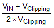
A differential input signal of 0 V ideally produces a stream of ones and zeros that are high 50% of the time. A differential input of 1 V produces a stream of ones and zeros that are high 90% of the time. With 16 bits of resolution, that percentage ideally corresponds to code 58982. A differential input of –1 V produces a stream of ones and zeros that are high 10% of the time and ideally results in code 6553 with 16-bit resolution. These input voltages are also the specified linear range of the AMC3336-Q1. If the input voltage value exceeds this range, the output of the modulator shows nonlinear behavior as the quantization noise increases. The output of the modulator clips with a stream of only zeros with an input less than or equal to –1.25 V or with a stream of only ones with an input greater than or equal to 1.25 V. In this case, however, the AMC3336-Q1 generates a single 1 (if the input is at negative full-scale) or 0 (if the input is at positive full-scale) every 128 clock cycles to indicate proper device function (see the Section 7.3.4.1 section for more details). Figure 7-4 shows the input voltage versus the output modulator signal.
 Figure 7-4 Analog
Input vs Modulator Output
Figure 7-4 Analog
Input vs Modulator OutputThe density of ones in the output bitstream for any input voltage value can be calculated using Equation 1 (with the exception of a full-scale input signal, as described in the Section 7.3.4.1 section):