SWRS202C May 2017 – January 2022 AWR1443
PRODUCTION DATA
- 1 Features
- 2 Applications
- 3 Description
- 4 Functional Block Diagram
- 5 Revision History
- 6 Device Comparison
- 7 Terminal Configuration and Functions
-
8 Specifications
- 8.1 Absolute Maximum Ratings
- 8.2 ESD Ratings
- 8.3 Power-On Hours (POH)
- 8.4 Recommended Operating Conditions
- 8.5 Power Supply Specifications
- 8.6 Power Consumption Summary
- 8.7 RF Specification
- 8.8 Thermal Resistance Characteristics for FCBGA Package [ABL0161]
- 8.9
Timing and Switching Characteristics
- 8.9.1 Power Supply Sequencing and Reset Timing
- 8.9.2 Synchronized Frame Triggering
- 8.9.3 Input Clocks and Oscillators
- 8.9.4
Multibuffered / Standard Serial Peripheral Interface (MibSPI)
- 8.9.4.1 Peripheral Description
- 8.9.4.2
MibSPI Transmit and Receive RAM Organization
- 8.9.4.2.1 SPI Timing Conditions
- 8.9.4.2.2 SPI Controller Mode Switching Parameters (CLOCK PHASE = 0, SPICLK = output, SPISIMO = output, and SPISOMI = input) (1) (1) (1)
- 8.9.4.2.3 SPI Controller Mode Switching Parameters (CLOCK PHASE = 1, SPICLK = output, SPISIMO = output, and SPISOMI = input) (1) (1) (1)
- 8.9.4.3 SPI Peripheral Mode I/O Timings
- 8.9.4.4 Typical Interface Protocol Diagram (Peripheral Mode)
- 8.9.5 LVDS Interface Configuration
- 8.9.6 General-Purpose Input/Output
- 8.9.7 Controller Area Network Interface (DCAN)
- 8.9.8 Serial Communication Interface (SCI)
- 8.9.9 Inter-Integrated Circuit Interface (I2C)
- 8.9.10 Quad Serial Peripheral Interface (QSPI)
- 8.9.11 JTAG Interface
- 9 Detailed Description
- 10Applications, Implementation, and Layout
- 11Device and Documentation Support
- 12Mechanical, Packaging, and Orderable Information
Package Options
Refer to the PDF data sheet for device specific package drawings
Mechanical Data (Package|Pins)
- ABL|161
Thermal pad, mechanical data (Package|Pins)
Orderable Information
9.7.2 Functional Mode
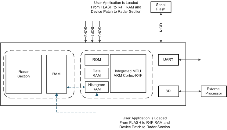
In Functional Mode, the Main System’s bootloader looks for a valid image in the serial flash memory, interfaced over the QSPI port. If a valid image is found, the bootloader transfers the same to Main System’s memory subsystem. If the device firmware image is found, it gets transferred to the Radar section’s memory subsystem.
If a valid image (or the QSPI Serial Flash is not found), the bootloader initializes the SPI port and awaits for the image transfer. This operation comes handy for configurations where the AWR1443 is interfaced to an external processor which has its own nonvolatile storage hence can store the user application and the AWR1443 device’s firmware image.
 Figure 9-8 Bootloader’s Functional Mode