SWRS273A november 2021 – march 2023 AWR2944
PRODUCTION DATA
- 1
- 1 Features
- 2 Applications
- 3 Description
- 4 Revision History
- 5 Device Comparison
- 6 Pin Configurations and Functions
-
7 Specifications
- 7.1 Absolute Maximum Ratings
- 7.2 ESD Ratings
- 7.3 Power-On Hours (POH)
- 7.4 Recommended Operating Conditions
- 7.5 VPP Specifications for One-Time Programmable (OTP) eFuses
- 7.6 Power Supply Specifications
- 7.7 Power Consumption Summary
- 7.8 RF Specifications
- 7.9 Thermal Resistance Characteristics
- 7.10 Power Supply Sequencing and Reset Timing
- 7.11 Input Clocks and Oscillators
- 7.12
Peripheral Information
- 7.12.1
QSPI Flash Memory Peripheral
- 7.12.1.1 QSPI Timing Conditions
- 7.12.1.2 QSPI Timing Requirements #GUID-CD30070D-F132-4A2C-92CD-5AA96AE70B94/GUID-97D19708-D87E-443B-9ADF-1760CFEF6F4C #GUID-CD30070D-F132-4A2C-92CD-5AA96AE70B94/GUID-0A61EEC9-2B95-4C27-B219-18D27C8F9430
- 7.12.1.3 QSPI Switching Characteristics #GUID-20B35D26-AFE6-451C-B9E9-B3F2FA08097C/T4362547-64 #GUID-20B35D26-AFE6-451C-B9E9-B3F2FA08097C/T4362547-65
- 7.12.2
Multibuffered / Standard Serial Peripheral Interface (MibSPI)
- 7.12.2.1 MibSPI Peripheral Description
- 7.12.2.2
MibSPI Transmit and Receive RAM Organization
- 7.12.2.2.1 SPI Timing Conditions
- 7.12.2.2.2 SPI Controller Mode Switching Parameters (CLOCK PHASE = 0, SPICLK = output, SPISIMO = output, and SPISOMI = input) #GUID-20BA2ACF-4FC2-43F6-960F-1A4CA56E65A6/T4362547-236 #GUID-20BA2ACF-4FC2-43F6-960F-1A4CA56E65A6/T4362547-237 #GUID-20BA2ACF-4FC2-43F6-960F-1A4CA56E65A6/T4362547-238
- 7.12.2.2.3 SPI Controller Mode Switching Parameters (CLOCK PHASE = 1, SPICLK = output, SPISIMO = output, and SPISOMI = input) #GUID-517E5284-3345-461F-B07F-EB95741B1272/T4362547-244 #GUID-517E5284-3345-461F-B07F-EB95741B1272/T4362547-245 #GUID-517E5284-3345-461F-B07F-EB95741B1272/T4362547-246
- 7.12.2.3 SPI Peripheral Mode I/O Timings
- 7.12.3
Ethernet Switch (RGMII/RMII/MII)
Peripheral
- 7.12.3.1 RGMII/MII Timing Conditions
- 7.12.3.2 RGMII Transmit Clock Switching Characteristics
- 7.12.3.3 RGMII Transmit Data and Control Switching Characteristics
- 7.12.3.4 RGMII Recieve Clock Timing Requirements
- 7.12.3.5 RGMII Receive Data and Control Timing Requirements
- 7.12.3.6 RMII Transmit Clock Switching Characteristics
- 7.12.3.7 RMII Transmit Data and Control Switching Characteristics
- 7.12.3.8 RMII Receive Clock Timing Requirements
- 7.12.3.9 RMII Receive Data and Control Timing Requirements
- 7.12.3.10 MII Transmit Switching Characteristics
- 7.12.3.11 MII Receive Clock Timing Requirements
- 7.12.3.12 MII Receive Timing Requirements
- 7.12.3.13 MII Transmit Clock Timing Requirements
- 7.12.3.14 MDIO Interface Timings
- 7.12.4 LVDS/Aurora Instrumentation and Measurement Peripheral
- 7.12.5 UART Peripheral
- 7.12.6 Inter-Integrated Circuit Interface (I2C)
- 7.12.7 Controller Area Network - Flexible Data-rate (CAN-FD)
- 7.12.8 CSI2 Receiver Peripheral
- 7.12.9 Enhanced Pulse-Width Modulator (ePWM)
- 7.12.10 General-Purpose Input/Output
- 7.12.1
QSPI Flash Memory Peripheral
- 7.13 Emulation and Debug
- 8 Detailed Description
- 9 Monitoring and Diagnostics
- 10Applications, Implementation, and Layout
- 11Device and Documentation Support
- 12Mechanical, Packaging, and Orderable Information
Package Options
Mechanical Data (Package|Pins)
- ALT|266
Thermal pad, mechanical data (Package|Pins)
Orderable Information
8.3.2 Processor Subsystem
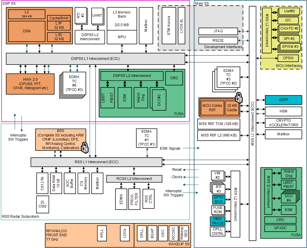
Figure 8-5 shows the block diagram for customer programmable processor subsystems in the device. At a high level there are two customer programmable subsystems. Left hand side shows the DSP Subsystem which contains TI's high performance C66x DSP, HWA 2.0, a high-bandwidth interconnect for high performance (128-bit, 150MHz), and associated peripherals – six EDMAs for data transfer,Aurora and LVDS interface for Measurement data output, L3 Radar data cube memory, ADC buffers, CRC engine, and data handshake memory (additional memory provided on interconnect).
For more information, see the TMS320C66x DSP CorePac User Guide
The right side of the diagram shows the Main subsystem (MSS). The Main subsystem, as the name suggests, is the primary controller of the device and controls all the device peripherals and house-keeping activities of the device. The Main subsystem contains a Cortex-R5F (MSS R5F) processor and associated peripherals and housekeeping components such as EDMAs, CRC, and peripherals (I2C, UART, SPIs, CAN-FD, EPWM, and others) connected to the primary interconnect through the Peripheral Central Resource (PCR interconnect).
The Radio Processing Subsystem or the BIST Subsystem (RSS) is responsible for initializing and calibrating the Analog/RF modules. RSS periodically monitors the Analog/RF functionality such that all the Analog/RF modules work in their defined limits.
General-Purpose ADC (GPADC), Fast Fourier Transformation engine (FFT engine) and other modules are provided to monitor the signal from different points in the transmitter and receiver chains. Digital front-end filters (DFE), Ramp Generation module and Analog/DFE registers, which are mainly under the control of BSS, can be indirectly controlled through the API calls from the Main Subsystem.
The device also integrates one two-lane CSI2 receiver interfaces in the radio processing subsystem. The prime functionality of this interface is the Hardware in loop (HIL) functionality, that can be used to perform the radar operations feeding the captured data from outside into the device without involving the RF subsystem.
Refer to the Device TRM (Technical Reference Manual) for MSS Cortex-R5F and DSP C66x memory map.
 Figure 8-5 Processor Subsystem