SLUSBY7 July 2014
PRODUCTION DATA.
- 1 Features
- 2 Applications
- 3 Description
- 4 Revision History
- 5 Description (Continued)
- 6 Pin Configuration and Functions
- 7 Specifications
-
8 Detailed Description
- 8.1 Overview
- 8.2 Functional Block Diagram
- 8.3 Feature Description
- 8.4
Device Functional Modes
- 8.4.1 Charge Profile
- 8.4.2 EN1/EN2 Pins
- 8.4.3 I2C Operation (Host Mode / Default Mode)
- 8.4.4 External Settings: ISET, ILIM and VIN_DPM
- 8.4.5 Transient Response
- 8.4.6 Input Voltage Based DPM
- 8.4.7 Sleep Mode
- 8.4.8 Input Over-Voltage Protection
- 8.4.9 NTC Monitor
- 8.4.10 Safety Timer
- 8.4.11 Watchdog Timer
- 8.4.12 Thermal Regulation and Thermal Shutdown
- 8.4.13 Fault Modes
- 8.4.14 Serial Interface Description
- 8.5 Register Maps
- 9 Application and Implementation
- 10Power Supply Recommendations
- 11Layout
- 12Device and Documentation Support
- 13Mechanical, Packaging, and Orderable Information
Package Options
Mechanical Data (Package|Pins)
- YFF|30
Thermal pad, mechanical data (Package|Pins)
Orderable Information
9 Application and Implementation
9.1 Application Information
The bq24250C is a high-efficiency switch-mode charger. The device has integrated power FETs that are able to charge at up to a 2-A charging rate, and an integrated 50-mA LDO. In I2C mode, the device has programmable battery charge voltage (VBATREG), charge current (ICHG), input current limit (ILIM), and input over-voltage protection threshold (VOVP). The charge current and the input current limit are programmed using external resistors (RISET and RILIM) connected from the ISET and ILIM pins to ground. The range of these resistors can be found in the datasheet. Both of these currents can be programmed up to 2 A. The device also has complete system-level protection such as input under-voltage lockout (UVLO), input over-voltage protection (OVP), battery OVP, sleep mode, thermal regulation and thermal shutdown, voltage-based NTC monitoring input, and safety timers.
9.2 Typical Application
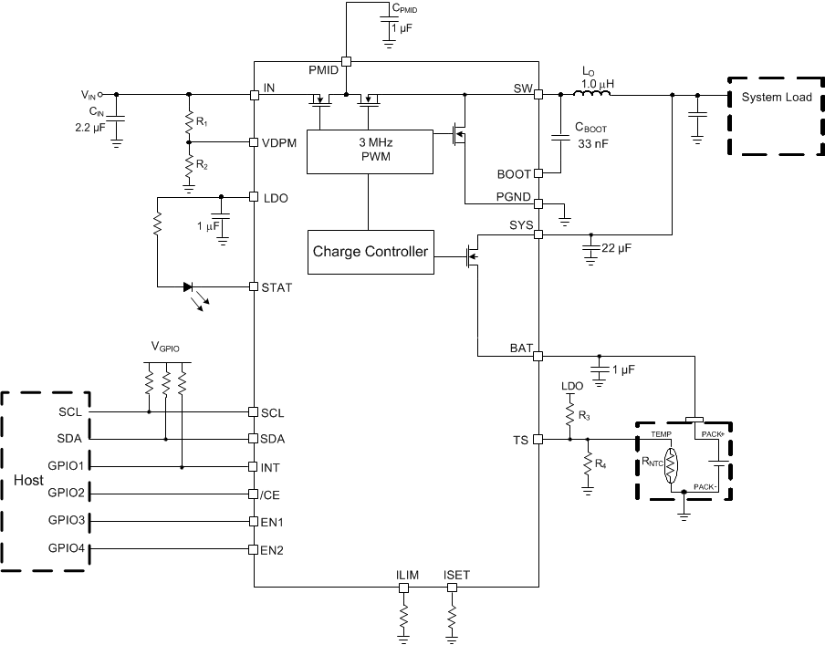 Figure 27. bq24250C Typical Application Circuit
9.2.1 Design Requirements
Use the following typical application design procedure to select external components values for the bq24250C device.
Table 4. Design Parameters
| SPECIFICATION | TEST CONDITION | MIN | TYP | MAX | UNIT |
|---|---|---|---|---|---|
| Input DC voltage, VIN | Recommended input voltage range | 4.35 | 10.5 | V | |
| Input current | Recommended input current range | 2 | A | ||
| Charge current | Fast charge current range | 0.5 | 2 | A | |
| Output regulation voltage | Standalone mode or I2C default mode | 4.2 | V | ||
| Output regulation voltage | I2C host mode: operating in voltage regulation, programmable range | 3.5 | 4.44 | V | |
| LDO | LDO output voltage | 4.9 | V |
9.2.2 Detailed Design Procedure
9.2.2.1 Inductor Selection
The inductor selection depends on the application requirements. The bq24250C is designed to operate at around 1 µH. The value will have an effect on efficiency, and the ripple requirements, stability of the charger, package size, and DCR of the inductor. The 1μH inductor provides a good tradeoff between size and efficiency and ripple.
Once the inductance has been selected, the peak current is needed in order to choose the saturation current rating of the inductor. Make sure that the saturation current is always greater than or equal to the calculated IPEAK. The following equation can be used to calculate the current ripple:
Then use current ripple to calculate the peak current as follows:
In this design example, the regulation voltage is set to 4.2V, the input voltage is 5V and the inductance is selected to be 1µH. The maximum charge current that can be used in this application is 1A and can be set by I2C command. The peak current is needed in order to choose the saturation current rating of the inductor. Using equation 6 and 7, ΔIL is calculated to be 0.224A and the inductor peak current is 1.112A. A 1µF BAT cap is needed and 22µF SYS cap is needed on the system trace.
The default settings for external fast charge current and external setting of current limit are chosen to be IFC=500mA and ILIM=1A. RISET and RILIM need to be calculated using equation 1 and 2 in the data sheet.
The fast charge current resistor (RISET) can be set as follows:
RISET=250/0.5A=500Ω
The input current limit resistor (RILIM) can be set as follows:
RILIM= 270/1A=270Ω
The external settings of VIN_DPM can be designed by calculating R1 and R2 according to equation 3 in this data sheet and the typical application circuit. VIN_DPM should be chosen first along with R1. VIN_DPM is chosen to be 4.48V and R1 is set to 274KΩ in this design example. Using equation 3, the value of R2 is calculated to be 100KΩ.
In this design example, the application needs to be JEITA compliant. Thus, TCOLD must be 0°C and THOT must be 60°C. If an NTC resistor is chosen such that the beta is 4500K and the nominal resistance is 13KΩ, the calculated R3 and R4 values are 5KΩ and 8.8KΩ respectively. These results are obtained from equation 4 and 5 in this data sheet.
9.2.3 Application Curves
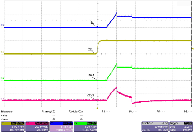
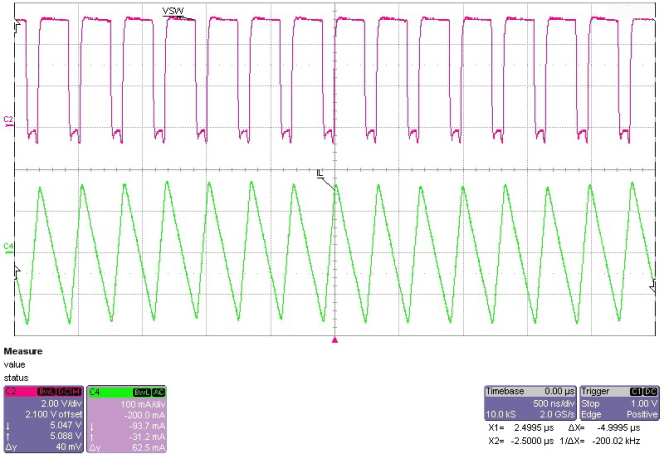
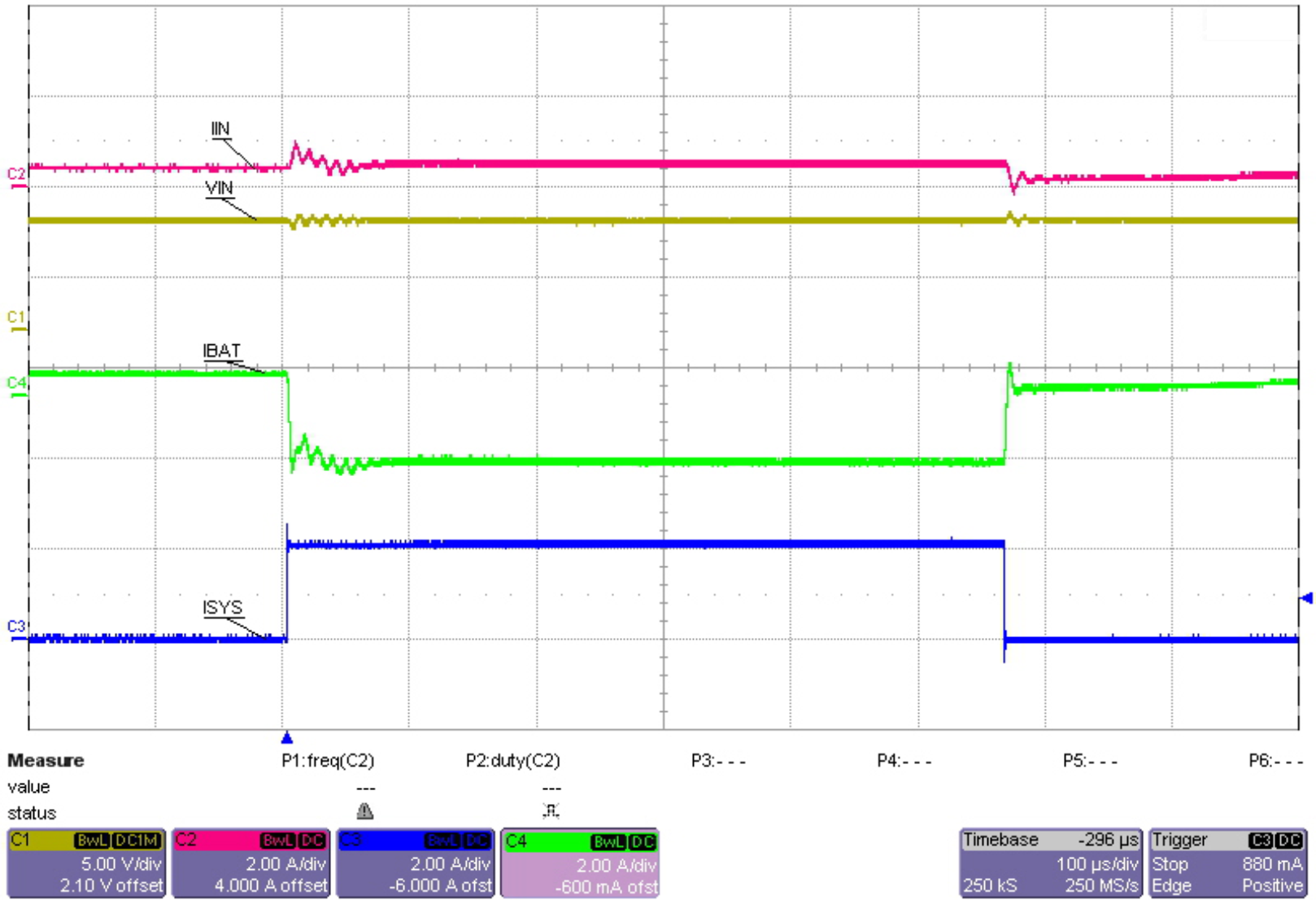 Figure 31. 2A Load Step Transient