SLUSBY7 July 2014
PRODUCTION DATA.
- 1 Features
- 2 Applications
- 3 Description
- 4 Revision History
- 5 Description (Continued)
- 6 Pin Configuration and Functions
- 7 Specifications
-
8 Detailed Description
- 8.1 Overview
- 8.2 Functional Block Diagram
- 8.3 Feature Description
- 8.4
Device Functional Modes
- 8.4.1 Charge Profile
- 8.4.2 EN1/EN2 Pins
- 8.4.3 I2C Operation (Host Mode / Default Mode)
- 8.4.4 External Settings: ISET, ILIM and VIN_DPM
- 8.4.5 Transient Response
- 8.4.6 Input Voltage Based DPM
- 8.4.7 Sleep Mode
- 8.4.8 Input Over-Voltage Protection
- 8.4.9 NTC Monitor
- 8.4.10 Safety Timer
- 8.4.11 Watchdog Timer
- 8.4.12 Thermal Regulation and Thermal Shutdown
- 8.4.13 Fault Modes
- 8.4.14 Serial Interface Description
- 8.5 Register Maps
- 9 Application and Implementation
- 10Power Supply Recommendations
- 11Layout
- 12Device and Documentation Support
- 13Mechanical, Packaging, and Orderable Information
Package Options
Mechanical Data (Package|Pins)
- YFF|30
Thermal pad, mechanical data (Package|Pins)
Orderable Information
7 Specifications
7.1 Absolute Maximum Ratings(1)
over operating free-air temperature range (unless otherwise noted)| MIN | MAX | UNIT | ||
|---|---|---|---|---|
| Pin Voltage (with respect to GND) | IN | –0.3 | 20 | V |
| SW | –0.7 | 12 | V | |
| BOOT | –0.3 | 20 | V | |
| LDO,STAT, INT, CHG, EN1, EN2, CE, ILIM, ISET, VDPM, TS | –0.3 | 7 | V | |
| SYS, BAT | –0.3 | 5 | V | |
| BOOT relative to SW | –0.3 | 7 | V | |
| Output Current (Continuous) | IN | 2 | A | |
| SYS, BAT | 4 | |||
| Output Sink Current | STAT, CHG | 5 | mA | |
| Operating free-air temperature | –40 | 85 | °C | |
| Junction temperature, TJ | –40 | 125 | °C | |
| Input Power | IN | 15 | W | |
(1) Stresses beyond those listed under absolute maximum ratings may cause permanent damage to the device. These are stress ratings only, and functional operation of the device at these or any other conditions beyond those indicated under recommended operating conditions is not implied. Exposure to absolute-maximum-rated conditions for extended periods may affect device reliability.
7.2 Handling Ratings
| MIN | MAX | UNIT | |||
|---|---|---|---|---|---|
| TSTG | Storage temperature range | –65 | 150 | °C | |
| V(ESD) | Electrostatic discharge | Human body model (HBM)(1) | 0 | 2000 | V |
(1) The human body model is a 100-pF capacitor discharged through a 1.5-kΩ resistor into each pin.
7.3 Recommended Operating Conditions
All voltages are with respect to PGND if not specified. Currents are positive into, negative out of the specified pin. Consult Packaging Section of the data book for thermal limitations and considerations of packages| MIN | MAX | UNIT | ||
|---|---|---|---|---|
| VIN | IN voltage range | 4.35 | 18(1) | V |
| IN operating voltage range | 4.35 | 10.5 | ||
| IIN | Input current | 2 | A | |
| ICHG | Current in charge mode, BAT | 2 | A | |
| IDISCHG | Current in discharge mode, BAT | 4 | A | |
| RISET | Charge current programming resistor range | 75 | Ω | |
| RILIM | Input current limit programming resistor range | 105 | Ω | |
| PIN | Input Power | 12 | W | |
| TJ | Operating junction temperature range | 0 | 125 | °C |
(1) The inherent switching noise voltage spikes should not exceed the absolute maximum rating on either the BOOT or SW pins. Small routing loops for the power nets in layout minimize switching noise.
7.4 Thermal Information
| THERMAL METRIC(1) | bq24250C | UNIT | ||
|---|---|---|---|---|
| YFF | RGE | |||
| RθJA | Junction-to-ambient thermal resistance | 76.5 | 32.9 | °C/W |
| RθJC(top) | Junction-to-case (top) thermal resistance | 0.2 | 32.8 | |
| RθJB | Junction-to-board thermal resistance | 44 | 10.6 | |
| ψJT | Junction-to-top characterization parameter | 1.6 | 0.3 | |
| ψJB | Junction-to-board characterization parameter | 43.4 | 10.7 | |
| RθJC(bot) | Junction-to-case (bottom) thermal resistance | N/A | 2.3 | |
(1) For more information about traditional and new thermal metrics, see the IC Package Thermal Metrics application report, SPRA953.
7.5 Electrical Characteristics
VUVLO < VIN < VOVP and VIN > VBAT+VSLP, TJ = 0ºC-125°C and TJ = 25°C for typical values (unless otherwise noted)| PARAMETER | TEST CONDITIONS | MIN | TYP | MAX | UNIT | |
|---|---|---|---|---|---|---|
| INPUT CURRENTS | ||||||
| IIN | Supply current from IN | VDPM < VIN < VOVP AND VIN > VBAT+VSLP PWM switching, CE Enable | 13 | mA | ||
| VDPM < VIN < VOVP AND VIN > VBAT+VSLP PWM switching, CE Disable | 5 | |||||
| 0°C< TJ < 85°C, High-Z Mode | 170 | 225 | μA | |||
| IBAT | Battery discharge current in high impedance mode, (BAT, SW, SYS) | 0°C< TJ < 85°C, VBAT = 4.2 V, VIN = 0V or 5V, High-Z Mode |
16 | 22 | μA | |
| Battery discharge current in SYSOFF mode, (BAT, SW, SYS) | 0°C< TJ < 85°C, VBAT = 4.2 V, VIN < UVLO, SYSOFF Mode |
1 | ||||
| POWER-PATH MANAGEMENT | ||||||
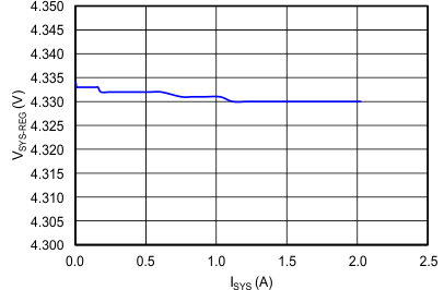
| VSYSREG | System Regulation Voltage | MINSYS stage (no DPM or DPPM) | –1% | 3.52 | 1% | V |
| MINSYS stage (DPM or DPPM active) | –1.50% | VMINSYS
–200mV |
1.50% | |||
| BATREG stage | VBAT
+ ICHG Ron |
|||||
| SYSREG stage | VBATREG
+2.1% |
VBATREG
+3.1% |
VBATREG
+4.1% |
|||
| VSPLM | Enter supplement mode voltage threshold | VBAT = 3.6V | VBAT – 40mV |
V | ||
| ISPLM | Exit supplement mode current threshold | VBAT = 3.6V | 20 | mA | ||
| BATTERY CHARGER | ||||||
| RON(BAT-SYS) | Internal battery charger MOSFET on-resistance | Measured from BAT to SYS, VBAT = 4.2V (WCSP) |
20 | 30 | mΩ | |
| VBATREG | I2C host mode | Operating in voltage regulation, Programmable Range | 3.5 | 4.44 | V | |
| SA mode or I2C default mode | 4.2 | |||||
| Voltage Regulation Accuracy | TJ = 25°C | –0.5% | 0.5% | |||
| TJ = 0°C to 125°C | –0.75% | 0.75% | ||||
| ICHG | Fast Charge Current Range | VLOWV ≤ VBAT < VBAT(REG) | 500 | 2000 | mA | |
| Fast Charge Current Accuracy | I2C mode | –7% | 7% | |||
| ICHG-LOW | Low Charge Current Setting | Set via I2C | 297 | 330 | 363 | mA |
| KISET | Programmable Fast Charge Current Factor |  |
232.5 | 250 | 267.5 | AΩ |
| VISET | Maximum ISET pin voltage (in regulation) | 0.39 | 0.42 | 0.45 | V | |
| RISET-SHORT | Short circuit resistance threshold | 40 | 55 | 75 | Ω | |
| VLOWV | Pre-charge to fast charge threshold | Rising | 2.9 | 3 | 3.1 | V |
| Hysteresis for VLOWV | Battery voltage falling | 100 | mV | |||
| IPRECHG | Pr-charge current (VBATUVLO < VBAT < VLOWV) | Ipre-chg is a precentile of the external fast charge settings. | 8% | 10 | 12% | |
| VBAT_UVLO | Battery Under voltage lockout threshold | VBAT rising | 2.39 | 2.52 | 2.65 | V |
| Battery UVLO hysteresis | 200 | mV | ||||
| VBATSHRT | Trickle charge to pre-charge threshold | 1.9 | 2 | 2.1 | V | |
| Hysteresis for VBATSHRT | Battery voltage falling | 100 | mV | |||
| IBATSHRT | Trickle charge mode charge current (VBAT < VBATSHRT) | 25 | 35 | 50 | mA | |
| ITERM | Termination Current Threshold | Termination current on SA only | 10 | %ICHG | ||
| Termination Current Threshold Tolerance | –10% | 10% | ||||
| VRCH | Recharge threshold voltage | Below VBATREG | 70 | 115 | 160 | mV |
| BATTERY DETECTION | ||||||
| VBATREG_HI | Battery Detection High Regulation Voltage | Same as VBATREG | VBATREG | V | ||
| VBATREG_LO | Battery Detection Low Regulation Voltage | 360 mV offset from VBATREG | VBATREG
–480mV |
V | ||
| VBATDET Hi | Battery detection comparator | VBATREG = VBATREG_HI | VBATREG
–120mV |
V | ||
| VBATDET LO | Battery detection comparator | VBATREG = VBATREG_LO | VBATREG
+120mV |
V | ||
| IDETECT | Battery Detection Current Sink | Always on during battery detection | 7.5 | mA | ||
| Tsafe | Safety Timer Accuracy | –10% | +10% | |||
| INPUT PROTECTION | ||||||
| IIN | Input current limiting | IIN_LIMIT = 100 mA | 90 | 95 | 100 | mA |
| IIN_LIMIT = 150 mA | 135 | 142.5 | 150 | |||
| IIN_LIMIT = 500 mA | 450 | 475 | 500 | |||
| IIN_LIMIT = 900 mA | 810 | 860 | 910 | |||
| IIN_LIMIT = 1500 mA | 1400 | 1475 | 1550 | |||
| IIN_LIMIT = 2000 mA | 1850 | 1950 | 2050 | |||
| IIN_LIMIT = External |  |
|||||
| ILIM | Maximum input current limit programmable range for IN input | 500 | 2000 | mA | ||
| KILIM | Maximum input current factor for IN input | ILIM = 500 mA to 2.0 A | 240 | 270 | 300 | AΩ |
| VILIM | Maximum ILIM pin voltage (in regulation) | 0.42 | V | |||
| RILIM-SHORT | Short circuit resistance threshold | 55 | 83 | 105 | Ω | |
| VIN_DPM | VIN_DPM threshold range | SA mode | 4.2 | 10 | V | |
| I2C mode | 4.2 | 4.76 | ||||
| VIN_DPM threshold for USB Input in SA mode | USB100, USB150, USB500, USB900, current limit selected. Also I2C register default. | 4.27 | 4.36 | 4.45 | ||
| VIN_DPM threshold with adaptor current limit and VDPM shorted to GND | Must set to external resistor settings via the EN1/EN2 pins or the I2C register interface. | VIN_DPM
–2% |
VIN_DPM | VIN_DPM
+2% |
||
| VIN_DPM threshold Accuracy | Both I2C and SA mode | –2% | 2% | |||
| VREF_DPM | DPM regulation voltage | External resistor setting only | 1.15 | 1.2 | 1.25 | V |
| VDPM_SHRT | VIN_DPM short threshold | If VDPM is shorted to ground, VIN_DPM threshold will use internal default value | 0.3 | V | ||
| VUVLO | IC active threshold voltage | VIN rising | 3.15 | 3.35 | 3.5 | V |
| IC active hysteresis | VIN falling from above VUVLO | 175 | mV | |||
| VSLP | Sleep-mode entry threshold, VIN-VBAT |
2.0 V ≤ VBAT ≤ VBATREG, VIN falling | 0 | 50 | 100 | mV |
| Sleep-mode exit hysteresis, VIN-VBAT |
2.0 V ≤ VBAT ≤ VBATREG | 40 | 100 | 160 | mV | |
| VOVP | Input supply OVP threshold voltage | IN rising | Input OVP –200mV |
Input OVP | Input OVP +200mV |
V |
| VOVP hysteresis | IN falling from VOVP | 100 | mV | |||
| VBOVP | Battery OVP threshold voltage | VBAT threshold over VBATREG to turn off charger during charge | 102.5 | 105 | 107.5 | % VBATREG |
| VBOVP hysteresis | Lower limit for VBAT falling from above VBOVP | 1 | % VBATREG | |||
| PWM CONVERTER | ||||||
| RON(BLK) | Internal blocking MOSFET on-resistance | Measured from IN to PMID | 60 | 100 | mΩ | |
| RON(HS) | Internal high-side MOSFET on-resistance | Measured from PMID to SW | 100 | 150 | mΩ | |
| RON(LS) | Internal low-side MOSFET on-resistance | Measured from SW to PGND | 110 | 165 | mΩ | |
| ICbC | Cycle-by-cycle current limit | VSYS shorted | 2.6 | 3.2 | 3.8 | A |
| fOSC | Oscillator frequency | 2.7 | 3 | 3.3 | MHz | |
| DMAX | Maximum duty cycle | 95% | ||||
| DMIN | Minimum duty cycle | 0% | ||||
| TSHTDWN | Thermal trip | 150 | °C | |||
| Thermal hysteresis | 10 | |||||
| TREG | Thermal regulation threshold | Charge current begins to cut off | 125 | |||
| LDO | ||||||
| VLDO | LDO Output Voltage | VIN = 5.5 V, ILDO = 0 to 50 mA | 4.65 | 4.95 | 5.25 | V |
| ILDO | Maximum LDO Output Current | 50 | mA | |||
| VDO | LDO Dropout Voltage (VIN – VLDO) | VIN = 5.0 V, ILDO = 50 mA | 200 | 300 | mV | |
| BATTERY-PACK NTC MONITOR (1) | ||||||
| VHOT | High temperature threshold | VTS falling | 29.6 | 30 | 30.4 | % VLDO |
| VHYS(HOT) | Hysteresis on high threshold | VTS rising | 0.6 | 0.9 | 1.2 | |
| VWARM | Warm temperature threshold | VTS falling | 37.9 | 38.3 | 38.7 | |
| VHYS(WARM) | Hysteresis on warm temperature threshold | VTS rising | 0.6 | 0.9 | 1.2 | |
| VCOOL | Cool temperature threshold | VTS rising | 48.1 | 48.5 | 48.9 | |
| VHSY(COOL) | Hysteresis on cool temperature threshold | VTS falling | 0.6 | 0.9 | 1.2 | |
| VCOLD | Low temperature threshold | VTS rising | 59.6 | 60 | 60.4 | |
| VHYS(COLD) | Hysteresis on low threshold | VTS falling | 0.6 | 0.9 | 1.2 | |
| VFRZ | Freeze temperature threshold | VTS rising | 62 | 62.5 | 63 | |
| VHYS(FRZ) | Hysteresis on freeze threshold | VTS falling | 0.6 | 0.9 | 1.2 | |
| ITS | TS current in charge mode | VIN = 5.0 V, VTS = 2.0 V, VBAT = 3.5 V | 0.005 | 0.1 | µA | |
| INPUTS (EN1, EN2, CE, SCL, SDA) | ||||||
| VIH | Input high threshold | 1 | V | |||
| VIL | Input low threshold | 0.4 | V | |||
| STATUS OUTPUTS (CHG, STAT, INT) | ||||||
| VOL | Low-level output saturation voltage | IO = 5 mA, sink current | 0.4 | V | ||
| IIH | High-level leakage current | Hi-Z and 5V applies | 1 | µA | ||
7.6 Timing Requirements
VUVLO < VIN < VOVP and VIN > VBAT+VSLP, TJ = 0ºC-125°C and TJ = 25°C for typical values (unless otherwise noted)| PARAMETER | TEST CONDITIONS | MIN | TYP | MAX | UNIT | |
|---|---|---|---|---|---|---|
| POWER-PATH MANAGEMENT | ||||||
| tDGL(SC1) | Deglitch Time, OUT Short Circuit during Discharge or Supplement Mode | Measured from (VBAT – VSYS) = 300 mV |
740 | μs | ||
| tREC(SC1) | Recovery Time, OUT Short Circuit during Discharge or Supplement Mode | 64 | ms | |||
| BATTERY CHARGER | ||||||
| tDGL(LOWV) | Deglitch time for pre-charge to fast charge transition | 32 | ms | |||
| tDGL(BATSHRT) | Deglitch time for trickle charge to pre-charge transition | 256 | µs | |||
| tDGL(TERM) | Deglitch time for charge termination | Both rising and falling, 2-mV over-drive, tRISE, tFALL = 100 ns | 64 | ms | ||
| tDGL(RCH) | Deglitch time | VBAT falling below VRCH, tFALL = 100 ns | 32 | ms | ||
| BATTERY DETECTION | ||||||
| tDETECT | Battery detection time | For both VBATREG_HI and VBATREG_LO | 32 | ms | ||
| INPUT PROTECTION | ||||||
| tDGL(SLP) | Deglitch time for IN rising above VIN+VSLP_EXIT | Rising voltage, 2-mV over drive, tRISE = 100 ns |
32 | ms | ||
| tDGL(OVP) | Deglitch time for IN Rising above VOVP | IN rising voltage, tRISE = 100 ns | 32 | ms | ||
| tDGL(BOVP) | BOVP Deglitch | Battery entering/exiting BOVP | 1 | ms | ||
| BATTERY-PACK NTC MONITOR (1) | ||||||
| tDGL(TS) | Deglitch time on TS change | 32 | ms | |||
| TIMERS | ||||||
| tSAFETY | 45 min safety timer | 2700 | s | |||
| 6 hr safety timer | 21600 | |||||
| 9 hr safety timer | 32400 | |||||
| tWATCH-DOG | Watch dog timer | 50 | s | |||
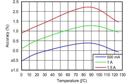
7.7 Typical Characteristics
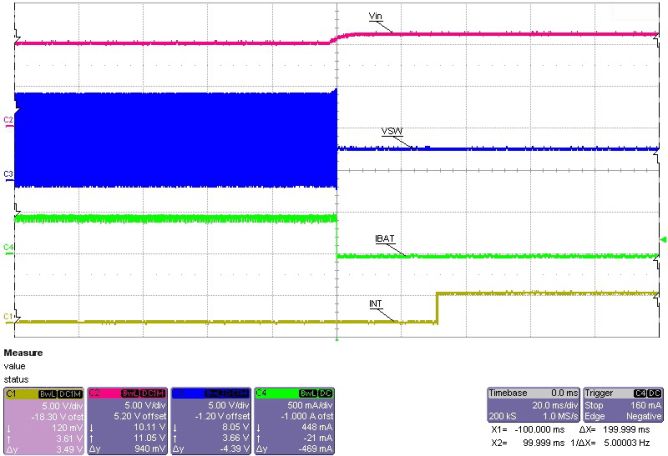
 Figure 1. Battery Detection
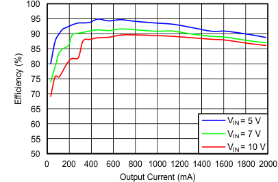
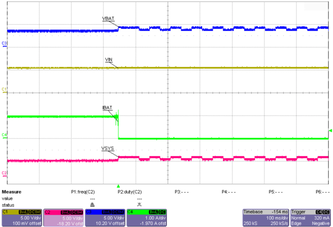 Figure 2. Battery Removal