SLUS892D December 2009 – December 2019 BQ24610 , BQ24617
PRODUCTION DATA.
- 1 Features
- 2 Applications
- 3 Description
- 4 Revision History
- 5 Description (continued)
- 6 Device Comparison Table
- 7 Pin Configuration and Functions
- 8 Specifications
-
9 Detailed Description
- 9.1 Overview
- 9.2 Functional Block Diagram
- 9.3
Feature Description
- 9.3.1 Battery Voltage Regulation
- 9.3.2 Battery Current Regulation
- 9.3.3 Input Adapter Current Regulation
- 9.3.4 Precharge
- 9.3.5 Charge Termination, Recharge, and Safety Timer
- 9.3.6 Power Up
- 9.3.7 Enable and Disable Charging
- 9.3.8 System Power Selector
- 9.3.9 Automatic Internal Soft-Start Charger Current
- 9.3.10 Converter Operation
- 9.3.11 Synchronous and Nonsynchronous Operation
- 9.3.12 Cycle-by-Cycle Charge Undercurrent Protection
- 9.3.13 Input Overvoltage Protection (ACOV)
- 9.3.14 Input Undervoltage Lockout (UVLO)
- 9.3.15 Battery Overvoltage Protection
- 9.3.16 Cycle-by-Cycle Charge Overcurrent Protection
- 9.3.17 Thermal Shutdown Protection
- 9.3.18 Temperature Qualification
- 9.3.19 Timer Fault Recovery
- 9.3.20 PG Output
- 9.3.21 CE (Charge Enable)
- 9.3.22 Charge Status Outputs
- 9.3.23 Battery Detection
- 9.4 Device Functional Modes
- 10Application and Implementation
- 11Power Supply Recommendations
- 12Layout
- 13Device and Documentation Support
- 14Mechanical, Packaging, and Orderable Information
Package Options
Mechanical Data (Package|Pins)
- RGE|24
Thermal pad, mechanical data (Package|Pins)
- RGE|24
Orderable Information
9.3.18 Temperature Qualification
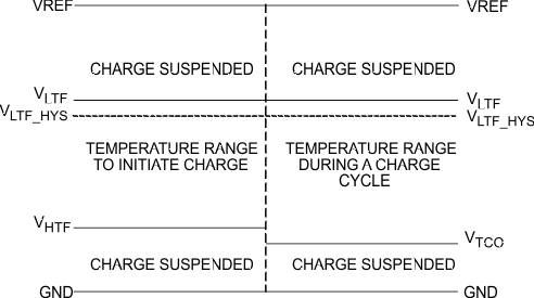
The controller continuously monitors battery temperature by measuring the voltage between the TS pin and GND. A negative temperature coefficient thermistor (NTC) and an external voltage divider typically develop this voltage. The controller compares this voltage against its internal thresholds to determine if charging is allowed. To initiate a charge cycle, the battery temperature must be within the VLTF to VHTF thresholds. If battery temperature is outside of this range, the controller suspends charge and the safety timer, and waits until the battery temperature is within the VLTF to VHTF range. During the charge cycle, the battery temperature must be within the VLTF to VTCO thresholds. If battery temperature is outside of this range, the controller suspends charge and waits until the battery temperature is within the VLTF to VHTF range. The controller suspends charge by turning off the PWM charge FETs. Figure 15 summarizes the operation.
 Figure 15. TS Pin, Thermistor Sense Thresholds
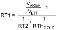
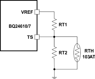
 Assuming a 103AT NTC thermistor on the battery pack as shown in Figure 20, the value RT1 and RT2 can be determined by using the following equations:


For example, 103AT NTC thermistors are used to monitor the battery pack temperature. Select TCOLD = 0ºC and TCUT_OFF = 45ºC; then we get RT2 = 430 kΩ, RT1 = 9.31 kΩ. A small RC filter is suggested to use for system-level ESD protection.
 Figure 16. TS Resistor Network