SLUS999A November 2009 – November 2015
PRODUCTION DATA.
- 1 Features
- 2 Applications
- 3 Description
- 4 Revision History
- 5 Description (Continued)
- 6 Pin Configuration and Functions
- 7 Specifications
-
8 Detailed Description
- 8.1 Overview
- 8.2 Functional Block Diagram
- 8.3
Feature Description
- 8.3.1 Adapter Detect and Power Up
- 8.3.2 Enable and Disable Charging
- 8.3.3 Automatic Internal Soft-Start Charger Current
- 8.3.4 Switching Frequency
- 8.3.5 Converter Operation
- 8.3.6 Refresh BTST Capacitor
- 8.3.7 UCP (Charge Undercurrent): Using Sense Resistor
- 8.3.8 Cycle-By-Cycle Charge Overcurrent Protection, Using High-Side Sense-FET
- 8.3.9 Average Charge Overcurrent Protection, Using Sense Resistor
- 8.3.10 Battery Overvoltage Protection, Using Remote Sensing VFB
- 8.3.11 Battery Short Protection
- 8.3.12 Battery Trickle Charging
- 8.3.13 High Accuracy VICM Using Current Sense Amplifier (CSA)
- 8.3.14 VDDSMB Input Supply
- 8.3.15 Input Undervoltage Lockout (UVLO)
- 8.3.16 VDDP Gate Drive Regulator
- 8.3.17 Input Current Comparator Trip Detection
- 8.3.18 Open-Drain Status Outputs (ACOK, ICOUT Pins)
- 8.3.19 Thermal Shutdown Protection
- 8.3.20 Charger Timeout
- 8.3.21 Charge Termination For Li-Ion or Li-Polymer
- 8.3.22 Remote Sense
- 8.4 Device Functional Modes
- 8.5 Programming
- 8.6 Register Maps
- 9 Application and Implementation
- 10Power Supply Recommendations
- 11Layout
- 12Device and Documentation Support
- 13Mechanical, Packaging, and Orderable Information
Package Options
Mechanical Data (Package|Pins)
- RUV|34
Thermal pad, mechanical data (Package|Pins)
- RUV|34
Orderable Information
1 Features
- Integrated Power MOSFETs, NMOS-NMOS, Synchronous Buck Converter
- >95% Efficiency
- Frequency 700kHz Allows Smaller Inductor (5 mm x 5 mm)
- Thermal Regulation Loop for Safety, Limit TJ = 120°C
- Adaptive Driver Dead-time and 99.5% Maximum Effective Duty Cycle
- High-Accuracy Voltage and Current Regulation
- ±0.5% Charge Voltage Accuracy
- ±3% Charge Current Accuracy
- ±3% Adapter Current Accuracy
- ±2% Input Current Sense Amp Accuracy
- Integration
- Integrated Power MOSFETs
- Input Current Comparator
- Internal Soft-Start
- Safety
- Thermal Regulation Loop and Thermal Shutdown
- Dynamic Power Management (DPM)
- Power FETs Over Current Protection
- 7 V–24 V AC/DC-Adapter Operating Range
- Simplified SMBus Control
- Charge Voltage DAC (1.024 V–19.2 V)
- Charge Current DAC (128 mA–8.064 A)
- Adapter Current Limit DPM DAC (256 mA–11.008 A)
- Status and Monitoring Outputs
- AC/DC Adapter Present With Adjustable Voltage Threshold
- Input Current Comparator, With Adjustable Threshold and Hysteresis
- Current Sense Amplifier for Current Drawn From Input Source
- Charge Any Battery Chemistry: Li+, LiFePO4, NiCd, NiMH, Lead Acid (2, 3, and 4 Li-Ion Cells)
- Charge Enable Pin (CE)
- Energy Star Low Iq
- < 10-μA Battery Current with Adapter Removed
- < 1 mA Input DCINA Current When Adapter Present and Charge Disabled
- 34-pin, 3.50 mm × 7.00 mm QFN Package
2 Applications
- Notebook and Ultra-Mobile Computers
- Portable Data-Capture Terminals
- Portable Printers
- Medical Diagnostics Equipment
- Battery Bay Chargers
- Battery Back-up Systems
3 Description
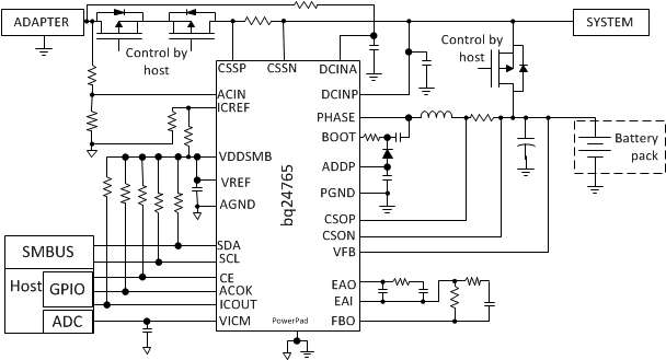
The bq24765 is a high-efficiency, synchronous battery charger with two integrated 30-mΩ NMOS power MOSFETs, and an integrated input current comparator, offering low component count for space-constraint, multi-chemistry battery charging applications. Input current, charge current, and charge voltage DACs allow for very high regulation accuracies that can be easily programmed by the system power management micro-controller using SMBus. The bq24765 has switching frequency of 700 kHz. The bq24765 charges 2, 3, or 4 series Li+ cells, and is available in a 34-pin, 3.50 mm x 7.00 mm VQFN package.
Device Information(1)
| PART NUMBER | PACKAGE | BODY SIZE (NOM) |
|---|---|---|
| bq24765 | VQFN (34) | 3.50 mm × 7.00 mm |
- For all available packages, see the orderable addendum at the end of the data sheet.
Simplified Schematic

4 Revision History
Changes from * Revision (November 2009) to A Revision
- Added ESD Ratings table, Feature Description section, Device Functional Modes, Application and Implementation section, Power Supply Recommendations section, Layout section, Device and Documentation Support section, and Mechanical, Packaging, and Orderable Information sectionGo
- Deleted Ordering Information table Go