SLUSBZ9C August   2015  – September 2016 BQ25120 , BQ25121

PRODUCTION DATA.  

  1. Features
  2. Applications
  3. Description
  4. Revision History
  5. Description (continued)
  6. Device Comparison Table
  7. Pin Configuration and Functions
  8. Specifications
    1. 8.1 Absolute Maximum Ratings
    2. 8.2 ESD Ratings
    3. 8.3 Recommended Operating Conditions
    4. 8.4 Thermal Information
    5. 8.5 Electrical Characteristics
    6. 8.6 Timing Requirements
    7. 8.7 Typical Characteristics
  9. Detailed Description
    1. 9.1 Overview
    2. 9.2 Functional Block Diagram
    3. 9.3 Feature Description
      1. 9.3.1  Ship Mode
      2. 9.3.2  High Impedance Mode
      3. 9.3.3  Active Battery Only Connected
      4. 9.3.4  Voltage Based Battery Monitor
      5. 9.3.5  Sleep Mode
      6. 9.3.6  Input Voltage Based Dynamic Power Management (VIN(DPM))
      7. 9.3.7  Input Overvoltage Protection and Undervoltage Status Indication
      8. 9.3.8  Battery Charging Process and Charge Profile
      9. 9.3.9  Dynamic Power Path Management Mode
      10. 9.3.10 Battery Supplement Mode
      11. 9.3.11 Default Mode
      12. 9.3.12 Termination and Pre-Charge Current Programming by External Components (IPRETERM)
      13. 9.3.13 Input Current Limit Programming by External Components (ILIM)
      14. 9.3.14 Charge Current Programming by External Components (ISET)
      15. 9.3.15 Safety Timer and Watchdog Timer
      16. 9.3.16 External NTC Monitoring (TS)
      17. 9.3.17 Thermal Protection
      18. 9.3.18 Typical Application Power Dissipation
      19. 9.3.19 Status Indicators (PG and INT)
      20. 9.3.20 Chip Disable (CD)
      21. 9.3.21 Buck (PWM) Output
      22. 9.3.22 Load Switch / LDO Output and Control
      23. 9.3.23 Manual Reset Timer and Reset Output (MR and RESET)
    4. 9.4 Device Functional Modes
    5. 9.5 Programming
      1. 9.5.1 Serial Interface Description
      2. 9.5.2 F/S Mode Protocol
    6. 9.6 Register Maps
      1. 9.6.1  Status and Ship Mode Control Register
      2. 9.6.2  Faults and Faults Mask Register
      3. 9.6.3  TS Control and Faults Masks Register
      4. 9.6.4  Fast Charge Control Register
      5. 9.6.5  Termination/Pre-Charge and I2C Address Register
      6. 9.6.6  Battery Voltage Control Register
      7. 9.6.7  SYS VOUT Control Register
      8. 9.6.8  Load Switch and LDO Control Register
      9. 9.6.9  Push-button Control Register
      10. 9.6.10 ILIM and Battery UVLO Control Register
      11. 9.6.11 Voltage Based Battery Monitor Register
      12. 9.6.12 VIN_DPM and Timers Register
  10. 10Application and Implementation
    1. 10.1 Application Information
    2. 10.2 Typical Application
      1. 10.2.1 Design Requirements
      2. 10.2.2 Detailed Design Procedure
        1. 10.2.2.1 Default Settings
        2. 10.2.2.2 Choose the Correct Inductance and Capacitance
        3. 10.2.2.3 Calculations
          1. 10.2.2.3.1 Program the Fast Charge Current (ISET)
          2. 10.2.2.3.2 Program the Input Current Limit (ILIM)
          3. 10.2.2.3.3 Program the Pre-charge/termination Threshold (IPRETERM)
          4. 10.2.2.3.4 TS Resistors (TS)
      3. 10.2.3 Application Performance Curves
        1. 10.2.3.1 Charger Curves
        2. 10.2.3.2 SYS Output Curves
        3. 10.2.3.3 Load Switch and LDO Curves
        4. 10.2.3.4 LS/LDO Output Curves
        5. 10.2.3.5 Timing Waveforms Curves
  11. 11Power Supply Recommendations
  12. 12Layout
    1. 12.1 Layout Guidelines
    2. 12.2 Layout Example
  13. 13Device and Documentation Support
    1. 13.1 Device Support
      1. 13.1.1 Third-Party Products Disclaimer
    2. 13.2 Related Links
    3. 13.3 Receiving Notification of Documentation Updates
    4. 13.4 Community Resources
    5. 13.5 Trademarks
    6. 13.6 Electrostatic Discharge Caution
    7. 13.7 Glossary
  14. 14Mechanical, Packaging, and Orderable Information

Package Options

Mechanical Data (Package|Pins)
Thermal pad, mechanical data (Package|Pins)
Orderable Information

8 Specifications

8.1 Absolute Maximum Ratings

over operating free-air temperature range (unless otherwise noted) (1)
MIN MAX UNIT
Input voltage IN wrt GND –0.3 20 V
PMID, VINLS wrt GND –0.3 7.7 V
CDSDA, SCL, ILIM, ISET, IPRETERM, LSCTRL, INT, RESET, TS wrt GND –0.3 5.5 V
Output voltage SYS 3.6 V
Input current IN 400 mA
Sink current INT 10 mA
Sink/Source Current RESET 10 mA
Output Voltage Continuos SW –0.7 7.7 V
Output Current Continuous SW 400 mA
SYS, BAT 300 mA
Current LS/LDO 150 mA
BAT Operating Voltage VBAT, MR, 6.6 V
Junction Temperature –40 125 °C
Storage Temperature, Tstg 300 °C
(1) Stresses beyond those listed under Absolute Maximum Ratings may cause permanent damage to the device. These are stress ratings only, which do not imply functional operation of the device at these or any other conditions beyond those indicated under Recommended Operating Conditions. Exposure to absolute-maximum-rated conditions for extended periods may affect device reliability.

8.2 ESD Ratings

VALUE UNIT
V(ESD) Electrostatic discharge Human body model (HBM), per ANSI/ESDA/JEDEC JS-001(1) ±2000 V
Charged device model (CDM), per JEDEC specification JESD22-C101(2) ±500
(1) JEDEC document JEP155 states that 500-V HBM allows safe manufacturing with a standard ESD control process.
(2) JEDEC document JEP157 states that 250-V CDM allows safe manufacturing with a standard ESD control process.

8.3 Recommended Operating Conditions

over operating free-air temperature range (unless otherwise noted)
MIN NOM MAX UNIT
VIN IN voltage range 3.4 5 20 V
IN operating voltage range, recommended 3.4 5 5.5
V(BAT) V(BAT) operating voltage range 5.5(1) V
V(VINLS) VINLS voltage range for Load Switch 0.8 5.5(2) V
V(VINLS) VINLS voltage range for LDO 2.2 5.5 V
IIN Input Current, IN input 400 mA
I(SW) Output Current from SW, DC 300 mA
I(PMID) Output Current from PMID, DC 300 mA
ILS/LDO Output Current from LS/LDO 100 mA
I(BAT), I(SYS) Charging and discharging using internal battery FET 300 mA
TJ Operating junction temperature range –40 125 °C
(1) Any voltage greater than shown should be a transient event.
(2) These inputs will support 6.6 V for less than 10% of the lifetime at V(BAT) or VIN, with a reduced current and/or performance.

8.4 Thermal Information

THERMAL METRIC(1) bq2512x UNIT
YFP (DSBGA)
25 PINS
RθJA Junction-to-ambient thermal resistance 60 °C/W
RθJC(top) Junction-to-case (top) thermal resistance 0.3 °C/W
RθJB Junction-to-board thermal resistance 12.0 °C/W
ψJT Junction-to-top characterization parameter 1.2 °C/W
ψJB Junction-to-board characterization parameter 12.0 °C/W
RθJC(bot) Junction-to-case (bottom) thermal resistance N/A °C/W
(1) For more information about traditional and new thermal metrics, see the IC Package Thermal Metrics application report, SPRA953.

8.5 Electrical Characteristics

Circuit of Figure 1, V(UVLO) < VIN < V(OVP) and VIN > V(BAT) + V(SLP), TJ = –40 to 85°C and TJ = 25°C for typical values (unless otherwise noted)
PARAMETERS TEST CONDITIONS MIN TYP MAX UNIT
INPUT CURRENTS
IIN Supply Current for Control V(UVLO) < VIN < V(OVP) and VIN > V(BAT) + V(SLP) PWM Switching, –40 < TJ < 85 1 mA
V(UVLO) < VIN < V(OVP) and VIN > V(BAT) + V(SLP) PWM NOT Switching 3 mA
0°C < TJ < 85°C, VIN = 5 V, Charge Disabled 1.5 mA
I(BAT_HIZ) Battery discharge current in High Impedance Mode 0°C < TJ < 60°C, VIN = 0 V, High-Z Mode, PWM Not Switching, V(BUVLO) < V(BAT) < 4.65V 0.7 1.2 µA
0°C < TJ < 60°C, VIN = 0 V, High-Z Mode, PWM Not Switching, V(BUVLO) < V(BAT) < 6.6 V 0.9 1.5 µA
0°C < TJ < 60°C, VIN = 0 V or floating, High-Z Mode, PWM Switching, No Load 0.75 3.5 µA
0°C < TJ < 85°C, VIN = 0 V, High-Z Mode, PWM Switching, LSLDO enabled 1.35 4.25 µA
I(BAT_ACTIVE) Battery discharge current in Active Battery Mode 0°C < TJ < 85°C, VIN = 0 V, Active Battery Mode, PWM Switching, LSLDO enabled, I2C Enabled, V(BUVLO) < V(BAT) < 4.65 V 6.8 12 µA
0°C < TJ < 85°C, 0 < VIN < VIN(UVLO), Active Battery Mode, PWM Switching, LSLDO disabled, I2C Enabled, /CD = Low, V(BUVLO) < V(BAT) < 4.65 V 6.2 11 µA
I(BAT_SHIP) Battery discharge current in Ship Mode 0°C < TJ < 85°C, VIN = 0 V, Ship Mode 2 150 nA
POWER-PATH MANAGEMENT and INPUT CURRENT LIMIT
VDO(IN-PMID) VIN – V(PMID) VIN = 5 V, IIN = 300 mA 125 170 mV
VDO(BAT-PMID) V(BAT) – V(PMID) VIN = 0 V, V(BAT) > 3 V, Iff = 400 mA 120 160 mV
V(BSUP1) Enter supplement mode threshold V(BAT) > V(BUVLO) V(PMID) < V(BAT) – 25 mV V
V(BSUP2) Exit supplement mode threshold V(BAT) > V(BUVLO) V(PMID) < V(BAT) – 5mV V
I(BAT_OCP) Current Limit, Discharge Mode V(BAT) > V(BUVLO) 0.85 1.15 1.35 A
I(ILIM) Input Current Limit Programmable Range, 50-mA steps 50 400 mA
Maximum Input Current using ILIM K(ILIM) / R(ILIM)
IILIM accuracy IILIM accuracy 50 mA to 100 mA –12% 12%
100 mA to 400 mA –5% 5%
K(ILIM) Maximum input current factor I(ILIM) = 50 mA to 100 mA 175 200 225
I(ILIM) = 100 mA to 400 mA 190 200 210
VIN(DPM) Input voltage threshold when input current is reduced Programmable Range using VIN(DPM) Registers. Can be disabled using VIN(DPM_ON) 4.2 4.9 V
VIN_DPM threshold accuracy –3% 3%
BATTERY CHARGER
VD(PPM) PMID voltage threshold when charge current is reduced Above V(BATREG) 0.2 V
RON(BAT-PMID) Internal Battery Charger MOSFET on-resistance Measured from BAT to PMID, V(BAT) = 4.35 V, High-Z mode 300 400
V(BATREG) Charge Voltage Operating in voltage regulation, Programmable Range, 10mV steps 3.6 4.65 V
Voltage Regulation Accuracy TJ = 25°C –0.5% 0.5%
TJ = 0°C to 85°C –0.5% 0.5%
I(CHARGE) Fast Charge Current Range V(BATUVLO) < V(BAT) < V(BATREG) 5 300 mA
Fast Charge Current using ISET K(ISET) / R(ISET) A
Fast Charge Current Accuracy –5% 5%
K(ISET) Fast Charge Current Factor 5 mA > I(CHARGE) > 300 mA 190 200 210
I(TERM) Termination charge current Termination current programmable range over I2C 0.5 37 mA
Termination Current using IPRETERM I(CHARGE) < 300 mA, R(ITERM) = 15 kΩ 5 % of ISET
I(CHARGE) < 300 mA, R(ITERM) = 4.99 kΩ 10 % of ISET
I(CHARGE) < 300 mA, R(ITERM) = 1.65 kΩ 15 % of ISET
I(CHARGE) < 300 mA, R(ITERM) = 549 Ω 20 % of ISET
Accuracy I(TERM) > 4 mA –10% 10%
tDGL(TERM) TERM deglitch time Both rising and falling, 2-mV over-drive, tRISE, tFALL = 100 ns 64 ms
I(PRE_CHARGE) Pre-charge current Pre-charge current programmable range over I2C 0.5 37 mA
Pre-charge Current using IPRETERM I(TERM) A
Accuracy –10% 10%
V(RCH) Recharge threshold voltage Below V(BATREG) 100 120 140 mV
tDGL(RCHG) Recharge threshold deglitch time tFALL = 100 ns typ, V(RCH) falling 32 ms
SYS OUTPUT
RDS(ON_HS) PMID = 3.6 V, I(SYS) = 50 mA 675 850
RDS(ON_LS) PMID = 3.6 V, I(SYS) = 50 mA 300 475
RDS(CH_SYS) MOSFET on-resistance for SYS discharge VIN = 3.6 V, IOUT = –10 mA into VOUT pin 22 40 Ω
I(LIMF) SW Current limit HS 2.2V < V(PMID) < 5.5 V 525 600 675 mA
SW Current limit LS 2.2V < V(PMID) < 5.5 V 525 700 850 mA
I(LIM_SS) PMOS switch current limit during softstart Current limit is reduced during softstart 80 130 200 mA
VSYS SYS Output Voltage Range Programmable range, 100 mV Steps 1.1 3.3 V
Output Voltage Accuracy VIN = 5 V, PFM mode, IOUT = 10 mA, V(SYS) = 1.8 V –2.5% 0 2.5%
DC Output Voltage Load Regulation in PWM mode VOUT = 2 V, Load range 0.01 %/mA
DC Output Voltage Line Regulation in PWM mode VOUT = 2.V, IOUT = 100 mA, VIN RANGE 0.01 %/V
LS/LDO OUTPUT
VIN(LS) Input voltage range for LS/LDO Load Switch Mode 0.8 6.6 V
Input voltage range for LS/LDO LDO Mode 2.2 6.6 V
VOUT DC output accuracy TJ = 25°C –2% ±1% 2%
Over VIN, IOUT, temperature –3% ±2% 3%
VLDO Output range for LS/LDO Programmable Range, 0.1 V steps 0.8 3.3 V
ΔVOUT / Δ VIN DC Line regulation VOUT(NOM) + 0.5 V < VIN < 6.6 V, IOUT = 5 mA –1% 1%
DC Load regulation 0 mA < IOUT < 100 mA –1% 1%
Load Transient 2 uA to 100 mA, VOUT = 1. 8V –120 60 mV
RDS(ON_LDO) FET Rdson V(VINLS) = 3.6 V 460 600
R(DSCH_LSLDO) MOSFET on-resistance for LS/LDO discharge 1.7V < V(VINLS) < 6.6 V, ILOAD = –10 mA 30 Ω
I(OCL_LDO) Output Current Limit – LDO VLS/LDO = 0.9 x VLS/LDO(NOM) 275 365 450 mA
I(LS/LDO) Output Current V(VINLS) = 3.6 V, VLSLDO = 3.3 V 100 mA
V(VINLS) = 3.3 V, VLSLDO = 0.8 V 100 mA
V(VINLS) = 2.2 V, VLSLDO = 0.8 V 10 mA
IIN(LDO) Quiescent current for VINLS in LDO mode 0.9 µA
OFF-state supply current 0.25 µA
VIH(LSCTRL) High-level input voltage for LSCTRL 1.15 V > V(VINLS) > 6.6 V 0.75 x V(SYS) 6.6 V
VIL(LSCTRL) Low-level input voltage for LSCTRL 1.15 V > V(VINLS) > 6.6 V 0.25 x V(SYS) V
PUSHBUTTON TIMER (MR)
VIL Low-level input voltage 0.3 V
RPU Internal pull-up resistance 120
VBAT MONITOR
VBMON Battery Voltage Monitor Accuracy V(BAT) Falling - Including 2% increment –3.5 3.5 %V(BATREG)
BATTERY-PACK NTC MONITOR
VHOT High temperature threshold VTS falling, 1% VIN Hysteresis bq25120 14.5 15 15.2 %VIN
bq25121
VWARM Warm temperature threshold VTS falling, 1% VIN Hysteresis bq25120 20.1 20.5 20.8 %VIN
bq25121 20.2 20.6 20.9
VCOOL Cool temperature threshold VTS rising, 1% VIN Hysteresis bq25120 35.4 36 36.4 %VIN
bq25121 35.5 36.1 36.5
VCOLD Low temperature threshold VTS rising, 1% VIN Hysteresis bq25120 39.3 39.8 40.2 %VIN
bq25121 39.5 40 40.3
TSOFF TS Disable threshold VTS rising, 2% VIN Hysteresis bq25120 55 60 %VIN
bq25121
PROTECTION
V(UVLO) IC active threshold voltage VIN rising 3.4 3.6 3.8 V
VUVLO(HYS) IC active hysteresis VIN falling from above VUVLO 150 mV
V(BUVLO) Battery Undervoltage Lockout threshold Range Programmable Range for V(BUVLO) VBAT falling, 200 mV Hysteresis 2.2 3.0 V
Default Battery Undervoltage Lockout Accuracy V(BAT) falling –2.5% 2.5%
V(BATSHORT) Battery short circuit threshold Battery voltage falling 2 V
V(BATSHORT_HYS) Hysteresis for V(BATSHORT) 100 mV
I(BATSHORT) Battery short circuit charge current I(PRETERM) mA
V(SLP) Sleep entry threshold, VIN – V(BAT) 2 V < VBAT < V(BATREG), VIN falling 65 120 mV
V(SLP_HYS) Sleep-mode exit hysteresis VIN rising above V(SLP) 40 65 100 mV
VOVP Maximum Input Supply OVP threshold voltage VIN rising, 100 mV hysteresis 5.35 5.55 5.75 V
tDGL_OVP Deglitch time, VIN OVP falling VIN falling below VOVP, 1V/us 32 ms
TSHTDWN Thermal trip VIN > VUVLO 114 °C
THYS Thermal hysteresis VIN > VUVLO 11 °C
tDGL_SHTDWN Deglitch time, Thermal shutdown TJ rising above TSHTDWN 4 µs
I2C INTERFACE
I2C Bus Specification standard and fast mode frequency support 100 400 kHz
VIL Input low threshold level VPULLUP = 1.1 V, SDA and SCL 0.275 V
VIH Input high threshold level VPULLUP = 1.1 V, SDA and SCL 0.825 V
VIH Input high threshold level VPULLUP = 3.3 V, SDA and SCL 2.475 V
VOL Output low threshold level IL = 5mA, sink current, VPULLUP = 1.1 V 0.275 V
IBIAS High-Level leakage current VPULLUP = 1.8V, SDA and SCL 1 µA
INT, PG, and RESET OUTPUT (Open Drain)
VOL Low level output threshold Sinking current = 5 mA 0.25 x V(SYS) V
IIN Bias current into pin Pin is high impedance, IOUT = 0 mA; TJ = –40°C to 60°C 12 nA
VIN(BAT_DELTA) Input voltage above VBAT where PG sends two 128 µs pulses each minute to signal the host of the input voltage status VUVLO < VIN < VOVP 0.825 1 1.15 V
INPUT PIN (CD LSCTRL)
VIL(/CD_LSCTRL) Input low threshold V(PULLUP) = 1V 0.25 V
VIH(/CD_LSCTRL) Input high threshold V(PULLUP) = 1V 0.75 V
RPULLDOWN/CD Internal pull-down resistance 900
R(LSCTRL) Internal pull-down resistance 2

8.6 Timing Requirements

MIN TYP MAX UNIT
POWER-PATH MANAGEMENT AND INPUT CURRENT LIMIT
tDGL_SC Deglitch Time, PMID or SW Short Circuit during Discharge Mode 250 µs
tREC_SC Recovery time, OUT Short Circuit during Discharge Mode 2 s
BATTERY CHARGER
tDGL_SHORT Deglitch time transition from ISET short to I(CHARGE) disable Clear fault by disconnecting VIN 1 ms
BATTERY CHARGING TIMERS
tMAXCHG Charge safety timer Programmable range 2 540 min
tPRECHG Precharge safety timer 0.1 x tMAXCHG
SYS OUTPUT
tONMIN Minimum ON time VIN = 3.6 V, VOUT = 2V, IOUT = 0 mA 225 ns
tOFFMIN Minimum OFF time VIN = 4.2 V 50 ns
tSTART_SW SW start up time VIN = 5 V, from write on EN_SW_OUT until output starts to rise 5 25 ms
tSTART_SYS SYS output time to start switching From insertion of BAT > V(BUVLO) or VIN > V(UVLO) 350 µs
tSOFTSTART Softstart time with reduced current limit 400 1200 µs
LS/LDO OUTPUT
tON_LDO Turn ON time 100mA load 500 µs
tOFF_LDO Turn OFF time 100mA load 5 µs
PUSHBUTTON TIMER
tWAKE1 Push button timer wake 1 Programmable Range for wake1 function 0.05 1 s
tWAKE2 Push button timer wake 2 Programmable Range for wake2 function 1 2 s
tRESET Push button timer reset Programmable Range for reset function 8 14 s
tRESET_D Reset pulse duration 400 ms
tDD Detection delay (from MR, input to RESET) For 0s condition 6 µs
BATTERY-PACK NTC MONITOR
tDGL(TS) Deglitch time on TS change Applies to V(HOT), V(WARM), V(COOL), and V(COLD) 50 ms
I2C INTERFACE
tWATCHDOG I2C interface reset timer for host 50 s
tI2CRESET I2C interface inactive reset timer 700 ms
tHIZ_ACTIVEBAT Transition time required to enable the I2C interface from HiZ to Active BAT 1 ms
INPUT PIN
t/CD_DGL Deglitch for CD CD rising/falling 100 µs
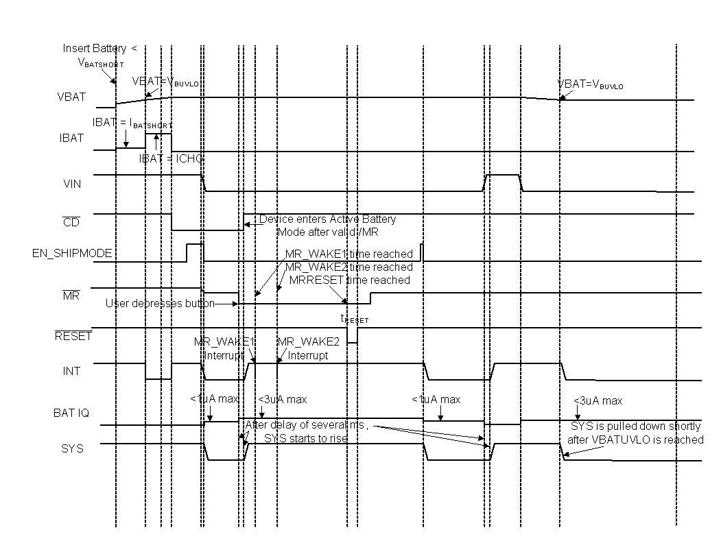
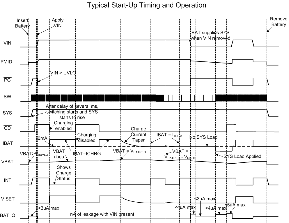
BQ25120 BQ25121 Startup_timing_slusbz9.gif
Conditions: PGB_MRS = 0, TE = 1, SW_LDO = 1, VINDPM_ON = 0, PG and INT pulled up to SYS, EN_INT = 1
Figure 1. Typical Start-Up Timing and Operation
BQ25120 BQ25121 battery_operation_timing_slusbz9.gif
Conditions: SW_LDO = 1, MRREC = 1, PG and INT pulled up to SYS, ISYS = 10 µA, EN_INT = 1
Figure 2. Battery Operation and Sleep Mode

8.7 Typical Characteristics
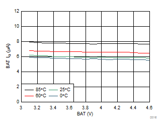
BQ25120 BQ25121 D016_SLUSBZ9.gif
Figure 3. Active BAT, IQ
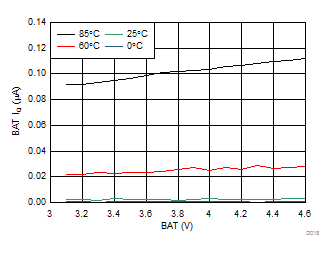
BQ25120 BQ25121 D018_SLUSBZ9.gif
Figure 5. Ship Mode BAT, IQ
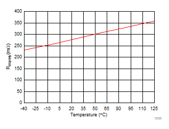
BQ25120 BQ25121 D025_SLUSBZ9.gif
Figure 7. Battery Discharge FET RDS(ON) vs Temperature
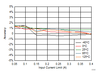
BQ25120 BQ25121 D020_SLUSBZ9.gif
Figure 9. ILIM Accuracy vs Input Current
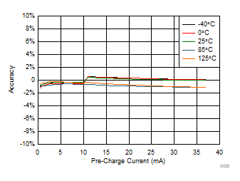
BQ25120 BQ25121 D022_SLUSBZ9.gif
Figure 11. Pre-Charge Accuracy vs Pre-Charge Current
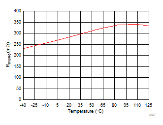
BQ25120 BQ25121 D027_SLUSBZ9.gif
VIN = 5 V
Figure 13. RDS(ON) of Low Side MOSFET vs Temperature
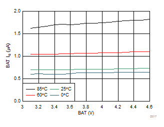
BQ25120 BQ25121 D017_SLUSBZ9.gif
1.8 V System Enabled (No Load)
Figure 4. Hi-Z BAT, IQ
BQ25120 BQ25121 D024_SLUSBZ9.gif
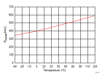
Figure 6. Blocking FET RDS(ON) vs Temperature
BQ25120 BQ25121 D019_SLUSBZ9.gif
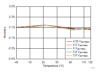
Figure 8. V(BATREG) Accuracy vs Temperature
BQ25120 BQ25121 D021_SLUSBZ9.gif
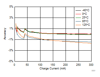
Figure 10. Charge Current Accuracy vs Charge Current
BQ25120 BQ25121 D026_SLUSBZ9.gif
VIN = 5 V
Figure 12. RDS(ON) of High Side MOSFET vs Temperature
BQ25120 BQ25121 D028_SLUSBZ9.gif
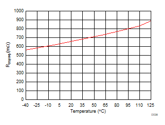
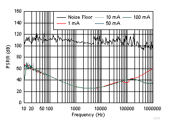
Figure 14. LS/LDO PSRR vs Frequency