SLUSE99C September   2021  – January 2023 BQ25180

PRODUCTION DATA  

  1. Features
  2. Applications
  3. Description
  4. Revision History
  5. Description (continued)
  6. Pin Configuration and Functions
  7. Specifications
    1. 7.1 Absolute Maximum Ratings
    2. 7.2 ESD Ratings
    3. 7.3 Thermal Information
    4. 7.4 Recommended Operating Conditions
    5. 7.5 Electrical Characteristics
    6. 7.6 Timing Requirements
    7. 7.7 Typical Characteristics
  8. Detailed Description
    1. 8.1 Overview
      1. 8.1.1 Battery Charging Process
        1. 8.1.1.1 Trickle Charge
        2. 8.1.1.2 Precharge
        3. 8.1.1.3 Fast Charge
        4. 8.1.1.4 Termination
    2. 8.2 Functional Block Diagram
    3. 8.3 Feature Description
      1. 8.3.1  Input Voltage Based Dynamic Power Management (VINDPM)
      2. 8.3.2  Dynamic Power Path Management Mode (DPPM)
      3. 8.3.3  Battery Supplement Mode
      4. 8.3.4  SYS Power Control (SYS_MODE bit control)
        1. 8.3.4.1 SYS Pulldown Control
      5. 8.3.5  SYS Regulation
      6. 8.3.6  ILIM Control
      7. 8.3.7  Protection Mechanisms
        1. 8.3.7.1 Input Overvoltage Protection
        2. 8.3.7.2 Battery Undervoltage Lockout
        3. 8.3.7.3 System Overvoltage Protection
        4. 8.3.7.4 System Short Protection
        5. 8.3.7.5 Battery Overcurrent Protection
        6. 8.3.7.6 Safety Timer and Watchdog Timer
        7. 8.3.7.7 Thermal Protection and Thermal Regulation
      8. 8.3.8  Pushbutton Wake and Reset Input
        1. 8.3.8.1 Pushbutton Wake or Short Button Press Functions
        2. 8.3.8.2 Pushbutton Reset or Long Button Press Functions
      9. 8.3.9  15-Second Timeout for HW Reset
      10. 8.3.10 Hardware Reset
      11. 8.3.11 Software Reset
      12. 8.3.12 Interrupt Indicator (/INT) Pin
      13. 8.3.13 External NTC Monitoring (TS)
        1. 8.3.13.1 TS Biasing and Function
      14. 8.3.14 I2C Interface
        1. 8.3.14.1 F/S Mode Protocol
    4. 8.4 Device Functional Modes
    5. 8.5 Register Maps
      1. 8.5.1 I2C Registers
  9. Application and Implementation
    1. 9.1 Application Information
    2. 9.2 Typical Application
      1. 9.2.1 Design Requirements
      2. 9.2.2 Detailed Design Procedure
        1. 9.2.2.1 Input (IN/SYS) Capacitors
        2. 9.2.2.2 TS
        3. 9.2.2.3 Recommended Passive Components
      3. 9.2.3 Application Curves
  10. 10Power Supply Recommendations
  11. 11Layout
    1. 11.1 Layout Guidelines
    2. 11.2 Layout Example
  12. 12Device and Documentation Support
    1. 12.1 Device Support
      1. 12.1.1 Third-Party Products Disclaimer
    2. 12.2 Receiving Notification of Documentation Updates
    3. 12.3 Support Resources
    4. 12.4 Trademarks
    5. 12.5 Electrostatic Discharge Caution
    6. 12.6 Glossary
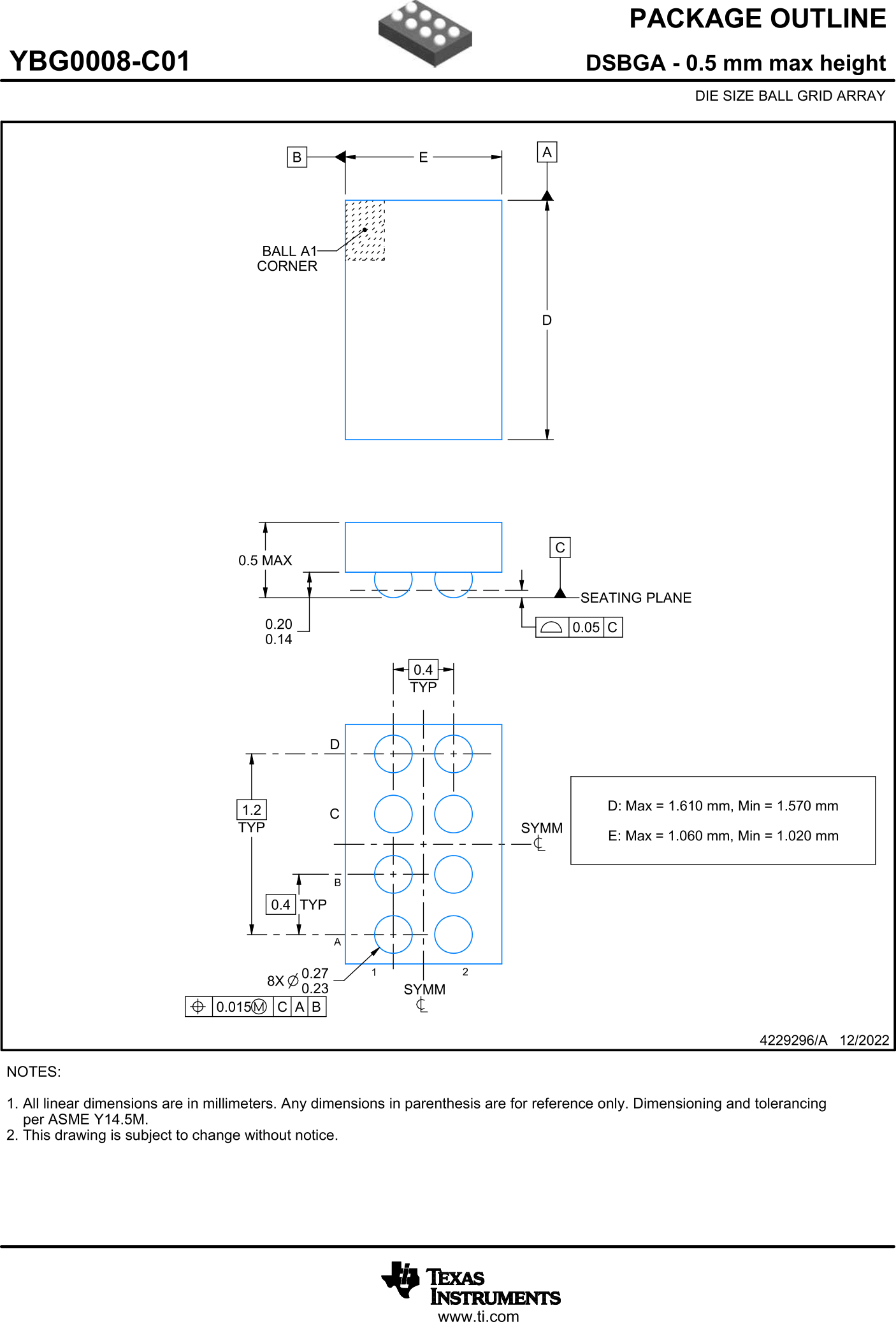
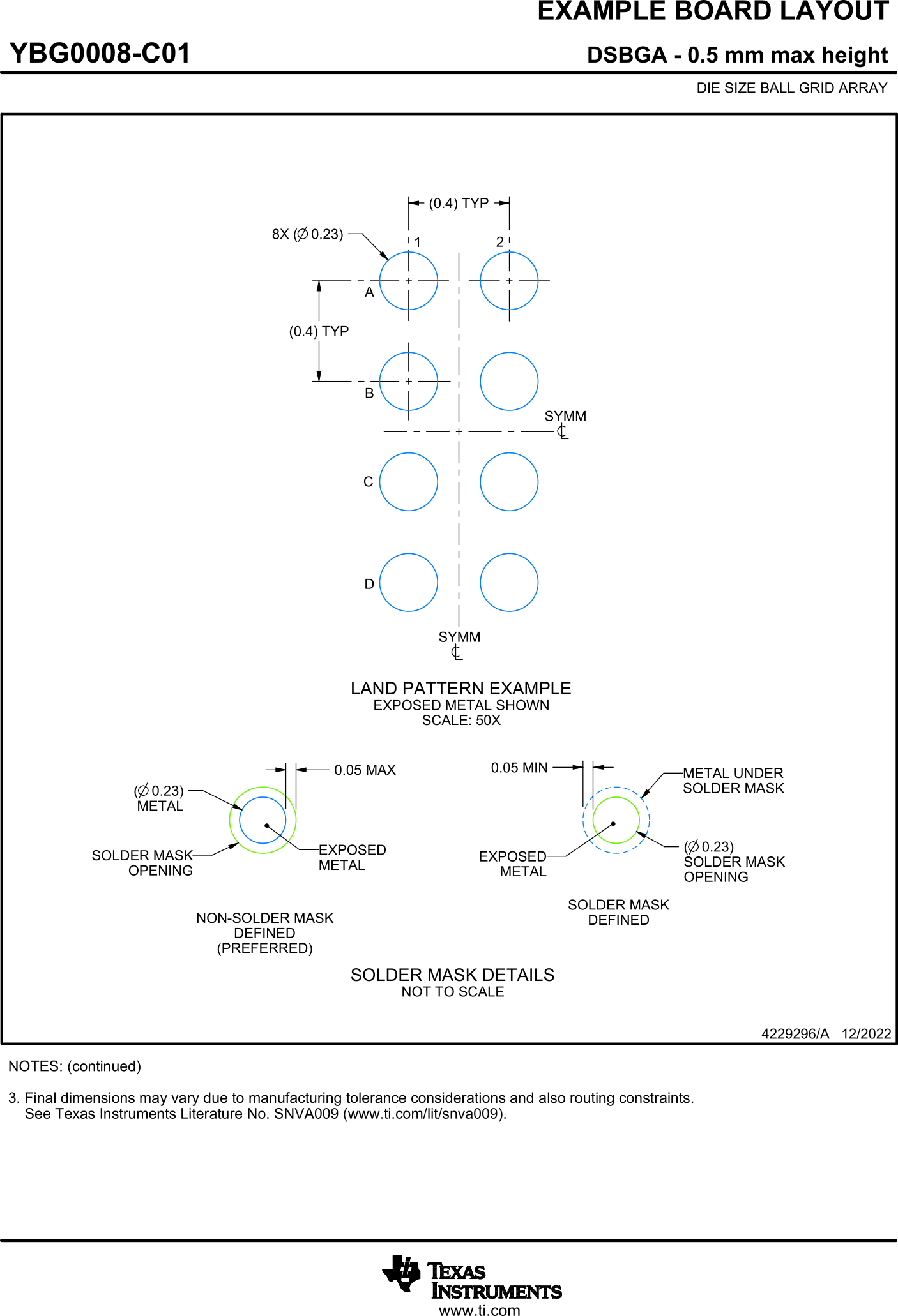
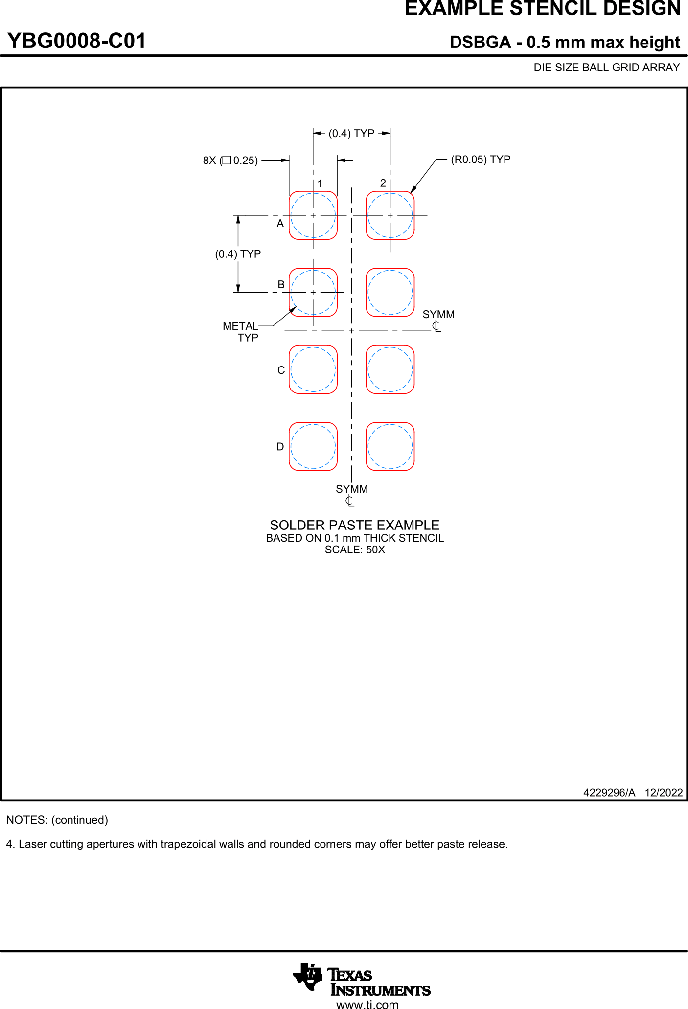
  13. 13Mechanical, Packaging, and Orderable Information

Package Options

Refer to the PDF data sheet for device specific package drawings

Mechanical Data (Package|Pins)
  • YBG|8
Thermal pad, mechanical data (Package|Pins)
Orderable Information

Mechanical, Packaging, and Orderable Information

The following pages include mechanical, packaging, and orderable information. This information is the most current data available for the designated devices. This data is subject to change without notice and revision of this document. For browser-based versions of this data sheet, refer to the left-hand navigation.

GUID-20221216-SS0I-VBBM-ZT4V-RSCX9BMZNWSD-low.gif
GUID-20221216-SS0I-NWG0-VHKR-JLW90C8XN1FZ-low.gif
GUID-20221216-SS0I-X9JB-F3MV-T1JS0RVLZJ5J-low.gif