SLUSDC7A March   2020  – November 2020 BQ25306

PRODUCTION DATA  

  1. Features
  2. Applications
  3. Description
  4. Revision History
  5. Description (continued)
  6. Device Comparison Table
  7. Pin Configuration and Functions
  8. Specifications
    1. 8.1 Absolute Maximum Ratings
    2. 8.2 ESD Ratings
    3. 8.3 Recommended Operating Conditions
    4. 8.4 Thermal Information
    5. 8.5 Electrical Characteristics
    6. 8.6 Timing Requirements
    7. 8.7 Typical Characteristics
  9. Detailed Description
    1. 9.1 Overview
    2. 9.2 Functional Block Diagram
    3. 9.3 Feature Description
      1. 9.3.1 Device Power Up
        1. 9.3.1.1 Power-On-Reset (POR)
        2. 9.3.1.2 REGN Regulator Power Up
        3. 9.3.1.3 Charger Power Up
        4. 9.3.1.4 Charger Enable and Disable by EN Pin
        5. 9.3.1.5 Device Unplugged from Input Source
      2. 9.3.2 Battery Charging Management
        1. 9.3.2.1 Battery Charging Profile
        2. 9.3.2.2 Precharge
        3. 9.3.2.3 Charging Termination
        4. 9.3.2.4 Battery Recharge
        5. 9.3.2.5 Charging Safety Timer
        6. 9.3.2.6 Thermistor Temperature Monitoring
      3. 9.3.3 Charging Status Indicator (STAT)
      4. 9.3.4 Protections
        1. 9.3.4.1 Voltage and Current Monitoring
          1. 9.3.4.1.1 Input Over-Voltage Protection
          2. 9.3.4.1.2 Input Voltage Dynamic Power Management (VINDPM)
          3. 9.3.4.1.3 Input Current Limit
          4. 9.3.4.1.4 Cycle-by-Cycle Current Limit
        2. 9.3.4.2 Thermal Regulation and Thermal Shutdown
        3. 9.3.4.3 Battery Protection
          1. 9.3.4.3.1 Battery Over-Voltage Protection (VBAT_OVP)
          2. 9.3.4.3.2 Battery Short Circuit Protection
        4. 9.3.4.4 ICHG Pin Open and Short Protection
    4. 9.4 Device Functional Modes
      1. 9.4.1 Disable Mode, HiZ Mode, Sleep Mode, Charge Mode, Termination Mode, and Fault Mode
  10. 10Application and Implementation
    1. 10.1 Application Information
    2. 10.2 Typical Applications
      1. 10.2.1 Typical Application
        1. 10.2.1.1 Design Requirements
        2. 10.2.1.2 Detailed Design Procedure
          1. 10.2.1.2.1 Charge Voltage Settings
          2. 10.2.1.2.2 Charge Current Setting
          3. 10.2.1.2.3 Inductor Selection
          4. 10.2.1.2.4 Input Capacitor
          5. 10.2.1.2.5 Output Capacitor
        3. 10.2.1.3 Application Curves
      2. 10.2.2 Typical Application with External Power Path
        1. 10.2.2.1 Design Requirements
      3. 10.2.3 Typical Application with MCU Programmable Charge Current
        1. 10.2.3.1 Design Requirements
  11. 11Power Supply Recommendations
  12. 12Layout
    1. 12.1 Layout Guidelines
    2. 12.2 Layout Example
  13. 13Device and Documentation Support
    1. 13.1 Device Support
      1. 13.1.1 Third-Party Products Disclaimer
    2. 13.2 Documentation Support
      1. 13.2.1 Related Documentation
    3. 13.3 Receiving Notification of Documentation Updates
    4. 13.4 Support Resources
    5. 13.5 Trademarks
    6. 13.6 Electrostatic Discharge Caution
    7. 13.7 Glossary
  14. 14Mechanical, Packaging, and Orderable Information

Package Options

Mechanical Data (Package|Pins)
Thermal pad, mechanical data (Package|Pins)
Orderable Information

Thermistor Temperature Monitoring

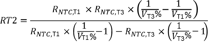
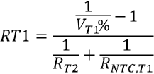
The charger device provides a single thermistor input TS pin for battery temperature monitor. RT1 and RT2 programs the cold temperature T1 and hot temperature T3. In the equations, RNTC,T1 is NTC thermistor resistance value at temperature T1 and RNTC,T3 is NTC thermistor resistance values at temperature T3. Assuming RHOT = 0, select 0°C to 45°C for battery charge temperature range, then NTC thermistor 103AT-2 resistance RNTC,T1 = 27.28 kΩ ( at 0°C) and RNTC,T3 = 4.91 kΩ (at 45°C), from the Equation 1 and Equation 2, RT1 and RT2 are derived as:

• RT1 = 4.527 kΩ

• RT2 = 23.26 kΩ

On top of the calculation results, adding RHOT resisitor can shift HOT temperature T3 up and only slightly shift up COLD temperature T1. The actual temperature T3 can be looked up in a NTC resistance table based on (RNTC,T3 - RHOT) and T1 can be looked up in a NTC resistance table based on (RNTC,T1 - RHOT). Because RNTC,T1 is much higher than RNTC,T3, RHOT can adjust HOT temperature significantly with mimimal affect on COLD temperature. RHOT is optional.

GUID-F893A799-4B8E-41F3-98EC-9CF4B8CFD30B-low.gifFigure 9-2 Battery Temperature Sensing Circuit
Equation 1. GUID-FD277864-6F3A-416A-A92D-06A735BB8429-low.gif
Equation 2. GUID-4C1FF4ED-DF10-4FF9-8795-AB0970A5B6FF-low.gif