SLUSDF8D June   2019  – December 2021 BQ25618 , BQ25619

PRODUCTION DATA  

  1. Features
  2. Applications
  3. Description
  4. Revision History
  5. Description (continued)
  6. Pin Configuration and Functions
  7. Specifications
    1. 7.1 Absolute Maximum Ratings
    2. 7.2 ESD Ratings
    3. 7.3 Recommended Operating Conditions
    4. 7.4 Thermal Information
    5. 7.5 Thermal Information
    6. 7.6 Electrical Characteristics
    7. 7.7 Timing Requirements
    8. 7.8 Typical Characteristics
  8. Detailed Description
    1. 8.1 Overview
    2. 8.2 Functional Block Diagram
    3. 8.3 Feature Description
      1. 8.3.1  Power-On-Reset (POR)
      2. 8.3.2  Device Power Up From Battery Without Input Source
      3. 8.3.3  Power Up From Input Source
        1. 8.3.3.1 Power Up REGN LDO
        2. 8.3.3.2 Poor Source Qualification
        3. 8.3.3.3 Input Source Type Detection (IINDPM Threshold)
          1. 8.3.3.3.1 PSEL Pins Sets Input Current Limit
        4. 8.3.3.4 Input Voltage Limit Threshold Setting (VINDPM Threshold)
        5. 8.3.3.5 Power Up Converter in Buck Mode
        6. 8.3.3.6 HIZ Mode with Adapter Present
      4. 8.3.4  Boost Mode Operation From Battery
      5. 8.3.5  Power Path Management
        1. 8.3.5.1 Narrow VDC Architecture
        2. 8.3.5.2 Dynamic Power Management
        3. 8.3.5.3 Supplement Mode
      6. 8.3.6  Battery Charging Management
        1. 8.3.6.1 Autonomous Charging Cycle
        2. 8.3.6.2 Battery Charging Profile
        3. 8.3.6.3 Charging Termination
        4. 8.3.6.4 Thermistor Qualification
          1. 8.3.6.4.1 JEITA Guideline Compliance During Charging Mode
          2. 8.3.6.4.2 Boost Mode Thermistor Monitor During Battery Discharge Mode
        5. 8.3.6.5 Charging Safety Timer
      7. 8.3.7  Ship Mode and QON Pin
        1. 8.3.7.1 BATFET Disable (Enter Ship Mode)
        2. 8.3.7.2 BATFET Enable (Exit Ship Mode)
        3. 8.3.7.3 BATFET Full System Reset
      8. 8.3.8  Status Outputs (STAT, INT , PMID_GOOD)
        1. 8.3.8.1 Power Good Indicator (PG_STAT Bit)
        2. 8.3.8.2 Charging Status Indicator (STAT)
        3. 8.3.8.3 Interrupt to Host (INT)
        4. 8.3.8.4 PMID Voltage Indicator (PMID_GOOD)
      9. 8.3.9  Protections
        1. 8.3.9.1 Voltage and Current Monitoring in Buck Mode
          1. 8.3.9.1.1 Input Overvoltage Protection (ACOV)
          2. 8.3.9.1.2 System Overvoltage Protection (SYSOVP)
        2. 8.3.9.2 Voltage and Current Monitoring in Boost Mode
          1. 8.3.9.2.1 Boost Mode Overvoltage Protection
          2. 8.3.9.2.2 PMID Overcurrent Protection
        3. 8.3.9.3 Thermal Regulation and Thermal Shutdown
          1. 8.3.9.3.1 Thermal Protection in Buck Mode
          2. 8.3.9.3.2 Thermal Protection in Boost Mode
        4. 8.3.9.4 Battery Protection
          1. 8.3.9.4.1 Battery Overvoltage Protection (BATOVP)
          2. 8.3.9.4.2 Battery Overdischarge Protection
          3. 8.3.9.4.3 System Overcurrent Protection
      10. 8.3.10 Serial Interface
        1. 8.3.10.1 Data Validity
        2. 8.3.10.2 START and STOP Conditions
        3. 8.3.10.3 Byte Format
        4. 8.3.10.4 Acknowledge (ACK) and Not Acknowledge (NACK)
        5. 8.3.10.5 Slave Address and Data Direction Bit
        6. 8.3.10.6 Single Read and Write
        7. 8.3.10.7 Multi-Read and Multi-Write
    4. 8.4 Device Functional Modes
      1. 8.4.1 Host Mode and Default Mode
    5. 8.5 Register Maps
  9. Application and Implementation
    1. 9.1 Application Information
    2. 9.2 Typical Application
      1. 9.2.1 Design Requirements
      2. 9.2.2 Detailed Design Procedure
        1. 9.2.2.1 Inductor Selection
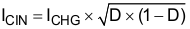
        2. 9.2.2.2 Input Capacitor and Resistor
        3. 9.2.2.3 Output Capacitor
      3. 9.2.3 Application Curves
  10. 10Power Supply Recommendations
  11. 11Layout
    1. 11.1 Layout Guidelines
    2. 11.2 Layout Example
  12. 12Device and Documentation Support
    1. 12.1 Device Support
      1. 12.1.1 Third-Party Products Disclaimer
    2. 12.2 Documentation Support
      1. 12.2.1 Related Documentation
    3. 12.3 Receiving Notification of Documentation Updates
    4. 12.4 Support Resources
    5. 12.5 Trademarks
    6. 12.6 Electrostatic Discharge Caution
    7. 12.7 Glossary
  13. 13Mechanical, Packaging, and Orderable Information

Package Options

Mechanical Data (Package|Pins)
Thermal pad, mechanical data (Package|Pins)
Orderable Information

Input Capacitor and Resistor

Design the input capacitance to provide enough ripple current rating to absorb the input switching ripple current. Worst case RMS ripple current is half of the charging current when the duty cycle is 0.5. If the converter does not operate at 50% duty cycle, then the worst case capacitor RMS current ICIN occurs where the duty cycle is closest to 50% and can be estimated using Equation 5.

Equation 5. GUID-129D9564-4889-4252-8787-3E2091DDD447-low.gif

A low ESR ceramic capacitor such as X7R or X5R is preferred for the input decoupling capacitor and should be placed as close as possible to the drain of the high-side MOSFET and source of the low-side MOSFET. The voltage rating of the capacitor must be higher than the normal input voltage level. A 25-V or higher rated capacitor is preferred for a 12-V input voltage. Minimum capacitance of 10 μF is suggested for typical of 1.5-A charging current.

During high current output over 700 mA in boost mode, a 10-kΩ pull-down resistor on VBUS is recommended to keep VBUS low in case Q1 RBFET leakage gets high.