SLUSEB9B december 2020 – july 2023 BQ25672
PRODUCTION DATA
- 1
- 1 Features
- 2 Applications
- 3 Description
- 4 Revision History
- 5 Description (continued)
- 6 Pin Configuration and Functions
- 7 Specifications
-
8 Detailed Description
- 8.1 Overview
- 8.2 Functional Block Diagram
- 8.3
Feature Description
- 8.3.1 Device Power-On-Reset
- 8.3.2 PROG Pin Configuration
- 8.3.3 Device Power Up from Battery without Input Source
- 8.3.4 Device Power Up from Input Source
- 8.3.5 Dual-Input Power Mux
- 8.3.6 Buck Converter Operation
- 8.3.7 USB On-The-Go (OTG)
- 8.3.8 Power Path Management
- 8.3.9 Battery Charging Management
- 8.3.10 Integrated 16-Bit ADC for Monitoring
- 8.3.11 Status Outputs ( STAT, and INT)
- 8.3.12 Ship FET Control
- 8.3.13
Protections
- 8.3.13.1
Voltage and Current Monitoring
- 8.3.13.1.1 VAC Over-voltage Protection (VAC_OVP)
- 8.3.13.1.2 VBUS Over-voltage Protection (VBUS_OVP)
- 8.3.13.1.3 VBUS Under-voltage Protection (POORSRC)
- 8.3.13.1.4 System Over-voltage Protection (VSYS_OVP)
- 8.3.13.1.5 System Short Protection (VSYS_SHORT)
- 8.3.13.1.6 Battery Over-voltage Protection (VBAT_OVP)
- 8.3.13.1.7 Battery Over-current Protection (IBAT_OCP)
- 8.3.13.1.8 Input Over-current Protection (IBUS_OCP)
- 8.3.13.1.9 OTG Over-voltage Protection (OTG_OVP)
- 8.3.13.1.10 OTG Under-voltage Protection (OTG_UVP)
- 8.3.13.2 Thermal Regulation and Thermal Shutdown
- 8.3.13.1
Voltage and Current Monitoring
- 8.3.14 Serial Interface
- 8.4 Device Functional Modes
- 8.5 Register Map
- 9 Application and Implementation
- 10Power Supply Recommendations
- 11Layout
- 12Device and Documentation Support
- 13Mechanical, Packaging, and Orderable Information
Package Options
Mechanical Data (Package|Pins)
- RQM|29
Thermal pad, mechanical data (Package|Pins)
Orderable Information
8.3.8.1 Narrow Voltage DC Architecture
The device deploys the NVDC architecture with a BATFET separating the system from the battery. Even with a fully depleted battery, the system is regulated above the minimum system voltage. The minimum system voltage is set by VSYSMIN bits. The default minimum system voltage at POR is determined according to different battery cell settings.
The NVDC architecture also provides the charging termination when the battery is fully charged. By turning off the BATFET, the adapter power is prioritized to support the system, which avoid the battery being continuously charged and discharged by the system load even if the adapter is present. This is very important to keep the battery in a healthy condition and extend the battery life time.
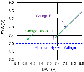
When the battery voltage is below the minimum system voltage setting, the BATFET operates in linear mode (LDO mode), and the system is regulated at around 200 mV above the minimum system voltage setting. As the battery voltage rises above the minimum system voltage, the BATFET is fully on and the voltage difference between the system and battery is the Rdson of BATFET multiplied by the charging current. When battery charging is disabled and VBAT is above the minimum system voltage setting or charging is terminated, the system is always regulated at typically 200mV (PFM disabled) or typical 600mV (PFM enabled) above battery voltage. The status register VSYS_STAT bit goes high when the system is in minimum system voltage regulation.
 Figure 8-7 Typical System Voltage vs Battery Voltage for a 2S Battery Configuration