SLUSEB9B december 2020 – july 2023 BQ25672
PRODUCTION DATA
- 1
- 1 Features
- 2 Applications
- 3 Description
- 4 Revision History
- 5 Description (continued)
- 6 Pin Configuration and Functions
- 7 Specifications
-
8 Detailed Description
- 8.1 Overview
- 8.2 Functional Block Diagram
- 8.3
Feature Description
- 8.3.1 Device Power-On-Reset
- 8.3.2 PROG Pin Configuration
- 8.3.3 Device Power Up from Battery without Input Source
- 8.3.4 Device Power Up from Input Source
- 8.3.5 Dual-Input Power Mux
- 8.3.6 Buck Converter Operation
- 8.3.7 USB On-The-Go (OTG)
- 8.3.8 Power Path Management
- 8.3.9 Battery Charging Management
- 8.3.10 Integrated 16-Bit ADC for Monitoring
- 8.3.11 Status Outputs ( STAT, and INT)
- 8.3.12 Ship FET Control
- 8.3.13
Protections
- 8.3.13.1
Voltage and Current Monitoring
- 8.3.13.1.1 VAC Over-voltage Protection (VAC_OVP)
- 8.3.13.1.2 VBUS Over-voltage Protection (VBUS_OVP)
- 8.3.13.1.3 VBUS Under-voltage Protection (POORSRC)
- 8.3.13.1.4 System Over-voltage Protection (VSYS_OVP)
- 8.3.13.1.5 System Short Protection (VSYS_SHORT)
- 8.3.13.1.6 Battery Over-voltage Protection (VBAT_OVP)
- 8.3.13.1.7 Battery Over-current Protection (IBAT_OCP)
- 8.3.13.1.8 Input Over-current Protection (IBUS_OCP)
- 8.3.13.1.9 OTG Over-voltage Protection (OTG_OVP)
- 8.3.13.1.10 OTG Under-voltage Protection (OTG_UVP)
- 8.3.13.2 Thermal Regulation and Thermal Shutdown
- 8.3.13.1
Voltage and Current Monitoring
- 8.3.14 Serial Interface
- 8.4 Device Functional Modes
- 8.5 Register Map
- 9 Application and Implementation
- 10Power Supply Recommendations
- 11Layout
- 12Device and Documentation Support
- 13Mechanical, Packaging, and Orderable Information
Package Options
Mechanical Data (Package|Pins)
- RQM|29
Thermal pad, mechanical data (Package|Pins)
Orderable Information
8.3.5.2 One ACFET-RBFET
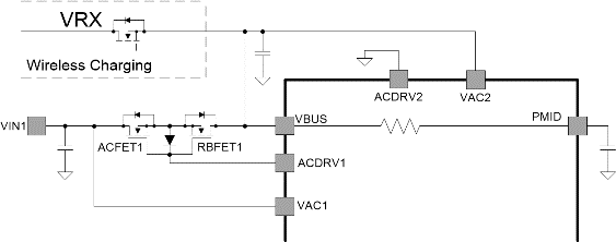
In this configuration, only ACFET1-RBFET1 is present, ACFET2-RBFET2 is not. VAC1 is tied to the drain of ACFET1, ACDRV1 is connected to the gate of ACFET1. VAC2 is shorted to VBUS, ACDRV2 is pulled down to GND. This structure is illustrated in the figure below, which is able to support either single input (one from VAC1 to VBUS through ACFET1-RBFET1, or one to VBUS directly) or dual-input (one from VAC1 to VBUS through ACFET1-RBFET1, the other one connected to VBUS directly) applications.
 Figure 8-3 One ACFET-RBFET Structure Supporting One Input at VAC1 and/or One Input at VBUS
- At POR, the charger detects only ACFET1-RBFET1 presented, updates ACRB1_STAT to 1 and keeps ACRB2_STAT as 0.
- The charger locks the register bit EN_ACDRV2 at 0, and the ACDRV2 pin will always stay low.
- When a valid input is presented at VAC1, the charger will set EN_ACDRV1 = 1 and turn ACFET1-RBFET1 on.
- To swap from the input at VAC1 to the input at VBUS, the host has to turn off the ACFET1-RBFET1 first by setting DIS_ACDRV=1 (forcing EN_ACDRV1 = 0), then enable the other input source which is connected to VBUS directly.
- In contrast, to swap from the input at VBUS to the input at VAC1, the host has to disable the input source connected to VBUS first, then turn on the ACFET1-RBFET1 by setting DIS_ACDRV = 0.