SLUSE66A June 2020 – January 2021 BQ25731
PRODUCTION DATA
- 1 Features
- 2 Applications
- 3 Description
- 4 Revision History
- 5 Description (continued)
- 6 Device Comparison Table
- 7 Pin Configuration and Functions
- 8 Specifications
-
9 Detailed Description
- 9.1 Overview
- 9.2 Functional Block Diagram
- 9.3
Feature Description
- 9.3.1 Power-Up Sequence
- 9.3.2 Two-Level Battery Discharge Current Limit
- 9.3.3 Fast Role Swap Feature
- 9.3.4 CHRG_OK Indicator
- 9.3.5 Input and Charge Current Sensing
- 9.3.6 Input Voltage and Current Limit Setup
- 9.3.7 Battery Cell Configuration
- 9.3.8 Device HIZ State
- 9.3.9 USB On-The-Go (OTG)
- 9.3.10 Converter Operation
- 9.3.11 Inductance Detection Through IADPT Pin
- 9.3.12 Converter Compensation
- 9.3.13 Continuous Conduction Mode (CCM)
- 9.3.14 Pulse Frequency Modulation (PFM)
- 9.3.15 Switching Frequency and Dithering Feature
- 9.3.16 Current and Power Monitor
- 9.3.17 Input Source Dynamic Power Management
- 9.3.18 Input Current Optimizer (ICO)
- 9.3.19 Two-Level Adapter Current Limit (Peak Power Mode)
- 9.3.20 Processor Hot Indication
- 9.3.21
Device Protection
- 9.3.21.1 Watchdog Timer
- 9.3.21.2 Input Overvoltage Protection (ACOV)
- 9.3.21.3 Input Overcurrent Protection (ACOC)
- 9.3.21.4 System Overvoltage Protection (SYSOVP)
- 9.3.21.5 Battery Overvoltage Protection (BATOVP)
- 9.3.21.6 Battery Discharge Overcurrent Protection (BATOC)
- 9.3.21.7 Battery Short Protection (BATSP)
- 9.3.21.8 System Undervoltage Lockout (VSYS_UVP)
- 9.3.21.9 Thermal Shutdown (TSHUT)
- 9.4 Device Functional Modes
- 9.5 Programming
- 9.6
Register Map
- 9.6.1 ChargeOption0 Register (I2C address = 01/00h) [reset = E70Eh]
- 9.6.2 ChargeCurrent Register (I2C address = 03/02h) [reset = 0080h]
- 9.6.3 ChargeVoltage Register (I2C address = 05/04h) [reset value based on CELL_BATPRESZ pin setting]
- 9.6.4 ChargerStatus Register (I2C address = 21/20h) [reset = 0000h]
- 9.6.5 ProchotStatus Register (I2C address = 23/22h) [reset = B800h]
- 9.6.6 IIN_DPM Register (I2C address = 25/24h) [reset = 4100h]
- 9.6.7 ADCVBUS/PSYS Register (I2C address = 27/26h)
- 9.6.8 ADCIBAT Register (I2C address = 29/28h)
- 9.6.9 ADCIIN/CMPIN Register (I2C address = 2B/2Ah)
- 9.6.10 ADCVSYS/VBAT Register (I2C address = 2D/2Ch)
- 9.6.11 ChargeOption1 Register (I2C address = 31/30h) [reset = 3F00h]
- 9.6.12 ChargeOption2 Register (I2C address = 33/32h) [reset = 00B7]
- 9.6.13 ChargeOption3 Register (I2C address = 35/34h) [reset = 0434h]
- 9.6.14 ProchotOption0 Register (I2C address = 37/36h) [reset = 4A81h(2S~5s) 4A09(1S)]
- 9.6.15 ProchotOption1 Register (I2C address = 39/38h) [reset = 41A0h]
- 9.6.16 ADCOption Register (I2C address = 3B/3Ah) [reset = 2000h]
- 9.6.17 ChargeOption4 Register (I2C address = 3D/3Ch) [reset = 0048h]
- 9.6.18 Vmin Active Protection Register (I2C address = 3F/3Eh) [reset = 006Ch(2s~5s)/0004h(1S)]
- 9.6.19 OTGVoltage Register (I2C address = 07/06h) [reset = 09C4h]
- 9.6.20 OTGCurrent Register (I2C address = 09/08h) [reset = 3C00h]
- 9.6.21 InputVoltage(VINDPM) Register (I2C address = 0B/0Ah) [reset =VBUS-1.28V]
- 9.6.22 IIN_HOST Register (I2C address = 0F/0Eh) [reset = 2000h]
- 9.6.23 ID Registers
- 10Application and Implementation
- 11Power Supply Recommendations
- 12Layout
- 13Device and Documentation Support
- 14Mechanical, Packaging, and Orderable Information
Package Options
Mechanical Data (Package|Pins)
- RSN|32
Thermal pad, mechanical data (Package|Pins)
- RSN|32
Orderable Information
10.2.2.1 Input Snubber and Filter for Voltage Spike Damping
During adapter hot plug-in, the parasitic inductance and input capacitor from the adapter cable form a second order system. The voltage spike at VBUS pin maybe beyond IC maximum voltage rating and damage IC. The input filter must be carefully designed and tested to prevent overvoltage event on VBUS pin.
There are several methods to damp or limit the overvoltage spike during adapter hot plug-in. An electrolytic capacitor with high ESR as an input capacitor can damp the overvoltage spike well below the IC maximum pin voltage rating. A high current capability TVS Zener diode can also limit the overvoltage level to an IC safe level. However these two solutions may not save cost or have small size.
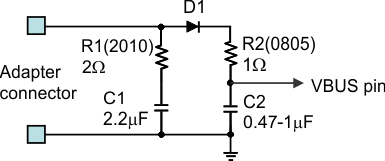
A cost effective and small size solution is shown in Figure 10-2. The R1 and C1 are composed of a damping RC network to damp the hot plug-in oscillation. As a result the over voltage spike is limited to a safe level. D1 is used for reverse voltage protection for VBUS pin. C2 is VBUS pin decoupling capacitor and it should be placed as close as possible to VBUS pin. C2 value should be less than C1 value so R1 can dominate the equivalent ESR value to get enough damping effect. R2 is used to limit inrush current of D1 to prevent D1 getting damage when adapter hot plug-in. R2 and C2 should have 10-µs time constant to limit the dv/dt on VBUS pin to reduce inrush current when adapter hot plug in. R1 has high inrush current. R1 package must be sized enough to handle inrush current power loss according to resistor manufacturer’s data sheet. The filter components' value always need to be verified with real application and minor adjustments may need to fit in the real application circuit.
 Figure 10-2 Input Filter