SLUSDG1C June   2020  – August 2022 BQ25792

PRODUCTION DATA  

  1. Features
  2. Applications
  3. Description
  4. Revision History
  5. Device Comparison
  6. Description (continued)
  7. Pin Configuration and Functions
  8. Specifications
    1. 8.1 Absolute Maximum Ratings
    2. 8.2 ESD Ratings
    3. 8.3 Recommended Operating Conditions
    4. 8.4 Thermal Information
    5. 8.5 Electrical Characteristics
    6. 8.6 Timing Requirements
    7. 8.7 Typical Characteristics
  9. Detailed Description
    1. 9.1 Overview
    2. 9.2 Functional Block Diagram
    3. 9.3 Feature Description
      1. 9.3.1  Device Power-On-Reset
      2. 9.3.2  PROG Pin Configuration
      3. 9.3.3  Device Power Up from Battery without Input Source
      4. 9.3.4  Device Power Up from Input Source
        1. 9.3.4.1 Power Up REGN LDO
        2. 9.3.4.2 Poor Source Qualification
        3. 9.3.4.3 ILIM_HIZ Pin
        4. 9.3.4.4 Default VINDPM Setting
        5. 9.3.4.5 Input Source Type Detection
          1. 9.3.4.5.1 D+/D– Detection Sets Input Current Limit
          2. 9.3.4.5.2 HVDCP Detection Procedure
          3. 9.3.4.5.3 Connector Fault Detection
      5. 9.3.5  Dual-Input Power Mux
        1. 9.3.5.1 ACDRV Turn On Condition
        2. 9.3.5.2 VBUS Input Only
        3. 9.3.5.3 One ACFET-RBFET
        4. 9.3.5.4 Two ACFETs-RBFETs
      6. 9.3.6  Buck-Boost Converter Operation
        1. 9.3.6.1 Force Input Current Limit Detection
        2. 9.3.6.2 Input Current Optimizer (ICO)
        3. 9.3.6.3 Pulse Frequency Modulation (PFM)
        4. 9.3.6.4 Device HIZ State
      7. 9.3.7  USB On-The-Go (OTG)
        1. 9.3.7.1 OTG Mode to Power External Devices
      8. 9.3.8  Power Path Management
        1. 9.3.8.1 Narrow VDC Architecture
        2. 9.3.8.2 Dynamic Power Management
      9. 9.3.9  Battery Charging Management
        1. 9.3.9.1 Autonomous Charging Cycle
        2. 9.3.9.2 Battery Charging Profile
        3. 9.3.9.3 Charging Termination
        4. 9.3.9.4 Charging Safety Timer
        5. 9.3.9.5 Thermistor Qualification
          1. 9.3.9.5.1 JEITA Guideline Compliance in Charge Mode
          2. 9.3.9.5.2 Cold/Hot Temperature Window in OTG Mode
      10. 9.3.10 Integrated 16-Bit ADC for Monitoring
      11. 9.3.11 Status Outputs ( STAT, and INT)
        1. 9.3.11.1 Charging Status Indicator (STAT Pin)
        2. 9.3.11.2 Interrupt to Host ( INT)
      12. 9.3.12 Ship FET Control
        1. 9.3.12.1 Shutdown Mode
        2. 9.3.12.2 Ship Mode
        3. 9.3.12.3 System Power Reset
      13. 9.3.13 Protections
        1. 9.3.13.1 Voltage and Current Monitoring
        2. 9.3.13.2 Thermal Regulation and Thermal Shutdown
      14. 9.3.14 Serial Interface
        1. 9.3.14.1 Data Validity
        2. 9.3.14.2 START and STOP Conditions
        3. 9.3.14.3 Byte Format
        4. 9.3.14.4 Acknowledge (ACK) and Not Acknowledge (NACK)
        5. 9.3.14.5 Target Address and Data Direction Bit
        6. 9.3.14.6 Single Write and Read
        7. 9.3.14.7 Multi-Write and Multi-Read
    4. 9.4 Device Functional Modes
      1. 9.4.1 Host Mode and Default Mode
      2. 9.4.2 Register Bit Reset
    5. 9.5 Register Map
      1. 9.5.1 I2C Registers
  10. 10Application and Implementation
    1. 10.1 Application Information
    2. 10.2 Typical Application
      1. 10.2.1 Design Requirements
      2. 10.2.2 Detailed Design Procedure
        1. 10.2.2.1 Inductor Selection
        2. 10.2.2.2 Input (VBUS / PMID) Capacitor
        3. 10.2.2.3 Output (VSYS) Capacitor
      3. 10.2.3 Application Curves
  11. 11Power Supply Recommendations
  12. 12Layout
    1. 12.1 Layout Guidelines
    2. 12.2 Layout Example
  13. 13Device and Documentation Support
    1. 13.1 Device Support
      1. 13.1.1 Third-Party Products Disclaimer
    2. 13.2 Documentation Support
      1. 13.2.1 Related Documentation
    3. 13.3 Receiving Notification of Documentation Updates
    4. 13.4 Support Resources
    5. 13.5 Trademarks
    6. 13.6 Electrostatic Discharge Caution
    7. 13.7 Glossary
  14. 14Mechanical, Packaging, and Orderable Information

Package Options

Mechanical Data (Package|Pins)
Thermal pad, mechanical data (Package|Pins)
Orderable Information

Output (VSYS) Capacitor

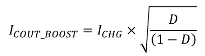
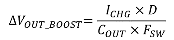
In the boost mode operation, the output current is discontinuous, which dominates the output RMS ripple current and output voltage ripple. The output capacitors should have enough ripple current rating to absorb the output AC current and have large enough capacitance to maintain the small output voltage ripple. For the boost mode operation, the output RMS ripple current is calculated by the equation (8) and the output voltage ripple is calculated by the equation (9), where D = (1 - VBUS / VSYS).

Equation 9. GUID-64907350-6170-44B4-AA4E-9369C4E82897-low.gif
Equation 10. GUID-FAB4B377-53AD-4715-9765-6C3F40084892-low.gif

The worst case output RMS ripple current and output voltage ripple both occur at the lowest VBUS input voltage. The SYS voltage is approximately 8V for the 2s battery configuration, so the worst case is 5V VBUS condition. Low ESR ceramic capacitor such as X7R or X5R is preferred for the output decoupling capacitor and should be placed close to the SYS and GND pins of the IC. The voltage rating of the capacitor must be higher than the normal input voltage level. The capacitor with 16V or higher voltage rating is preferred for the 2s battery configuration. 1*0.1 μF + 5*10 μF capacitors are suggested for up to 5A charging current.