SLUSDV2B May   2020  – January 2023 BQ25798

PRODUCTION DATA  

  1. Features
  2. Applications
  3. Description
  4. Revision History
  5. Description (continued)
  6. Device Comparison
  7. Pin Configuration and Functions
  8. Specifications
    1. 8.1 Absolute Maximum Ratings
    2. 8.2 ESD Ratings
    3. 8.3 Recommended Operating Conditions
    4. 8.4 Thermal Information
    5. 8.5 Electrical Characteristics
    6. 8.6 Timing Requirements
    7. 8.7 Typical Characteristics
  9. Detailed Description
    1. 9.1 Overview
    2. 9.2 Functional Block Diagram
    3. 9.3 Feature Description
      1. 9.3.1  Device Power-On-Reset
      2. 9.3.2  PROG Pin Configuration
      3. 9.3.3  Device Power Up from Battery without Input Source
      4. 9.3.4  Device Power Up from Input Source
        1. 9.3.4.1 Power Up REGN LDO
        2. 9.3.4.2 Poor Source Qualification
        3. 9.3.4.3 ILIM_HIZ Pin
        4. 9.3.4.4 Default VINDPM Setting
        5. 9.3.4.5 Input Source Type Detection
          1. 9.3.4.5.1 D+/D– Detection Sets Input Current Limit
          2. 9.3.4.5.2 HVDCP Detection Procedure
          3. 9.3.4.5.3 Connector Fault Detection
      5. 9.3.5  Dual-Input Power Mux
        1. 9.3.5.1 ACDRV Turn On Condition
        2. 9.3.5.2 VBUS Input Only
        3. 9.3.5.3 One ACFET-RBFET
        4. 9.3.5.4 Two ACFETs-RBFETs
      6. 9.3.6  Buck-Boost Converter Operation
        1. 9.3.6.1 Force Input Current Limit Detection
        2. 9.3.6.2 Input Current Optimizer (ICO)
        3. 9.3.6.3 Maximum Power Point Tracking for Small PV Panel
        4. 9.3.6.4 Pulse Frequency Modulation (PFM)
        5. 9.3.6.5 Device HIZ State
      7. 9.3.7  USB On-The-Go (OTG)
        1. 9.3.7.1 OTG Mode to Power External Devices
        2. 9.3.7.2 Backup Power Supply Mode
        3. 9.3.7.3 Backup Mode with Dual Input Mux
      8. 9.3.8  Power Path Management
        1. 9.3.8.1 Narrow VDC Architecture
        2. 9.3.8.2 Dynamic Power Management
      9. 9.3.9  Battery Charging Management
        1. 9.3.9.1 Autonomous Charging Cycle
        2. 9.3.9.2 Battery Charging Profile
        3. 9.3.9.3 Charging Termination
        4. 9.3.9.4 Charging Safety Timer
        5. 9.3.9.5 Thermistor Qualification
          1. 9.3.9.5.1 JEITA Guideline Compliance in Charge Mode
          2. 9.3.9.5.2 Cold/Hot Temperature Window in OTG Mode
      10. 9.3.10 Integrated 16-Bit ADC for Monitoring
      11. 9.3.11 Status Outputs ( STAT, and INT)
        1. 9.3.11.1 Charging Status Indicator (STAT Pin)
        2. 9.3.11.2 Interrupt to Host ( INT)
      12. 9.3.12 Ship FET Control
        1. 9.3.12.1 Shutdown Mode
        2. 9.3.12.2 Ship Mode
        3. 9.3.12.3 System Power Reset
      13. 9.3.13 Protections
        1. 9.3.13.1 Voltage and Current Monitoring
          1. 9.3.13.1.1  VAC Over-voltage Protection (VAC_OVP)
          2. 9.3.13.1.2  VBUS Over-voltage Protection (VBUS_OVP)
          3. 9.3.13.1.3  VBUS Under-voltage Protection (POORSRC)
          4. 9.3.13.1.4  System Over-voltage Protection (VSYS_OVP)
          5. 9.3.13.1.5  System Short Protection (VSYS_SHORT)
          6. 9.3.13.1.6  Battery Over-voltage Protection (VBAT_OVP)
          7. 9.3.13.1.7  Battery Over-current Protection (IBAT_OCP)
          8. 9.3.13.1.8  Input Over-current Protection (IBUS_OCP)
          9. 9.3.13.1.9  OTG Over-voltage Protection (OTG_OVP)
          10. 9.3.13.1.10 OTG Under-voltage Protection (OTG_UVP)
        2. 9.3.13.2 Thermal Regulation and Thermal Shutdown
      14. 9.3.14 Serial Interface
        1. 9.3.14.1 Data Validity
        2. 9.3.14.2 START and STOP Conditions
        3. 9.3.14.3 Byte Format
        4. 9.3.14.4 Acknowledge (ACK) and Not Acknowledge (NACK)
        5. 9.3.14.5 Target Address and Data Direction Bit
        6. 9.3.14.6 Single Write and Read
        7. 9.3.14.7 Multi-Write and Multi-Read
    4. 9.4 Device Functional Modes
      1. 9.4.1 Host Mode and Default Mode
      2. 9.4.2 Register Bit Reset
    5. 9.5 Register Map
      1. 9.5.1 I2C Registers
  10. 10Application and Implementation
    1. 10.1 Application Information
    2. 10.2 Typical Application
      1. 10.2.1 Design Requirements
      2. 10.2.2 Detailed Design Procedure
        1. 10.2.2.1 PV Panel Selection
        2. 10.2.2.2 Inductor Selection
        3. 10.2.2.3 Input (VBUS / PMID) Capacitor
        4. 10.2.2.4 Output (VSYS) Capacitor
      3. 10.2.3 Application Curves
  11. 11Power Supply Recommendations
  12. 12Layout
    1. 12.1 Layout Guidelines
    2. 12.2 Layout Example
  13. 13Device and Documentation Support
    1. 13.1 Device Support
      1. 13.1.1 Third-Party Products Disclaimer
    2. 13.2 Documentation Support
      1. 13.2.1 Related Documentation
    3. 13.3 Receiving Notification of Documentation Updates
    4. 13.4 Support Resources
    5. 13.5 Trademarks
    6. 13.6 Electrostatic Discharge Caution
    7. 13.7 Glossary
  14. 14Mechanical, Packaging, and Orderable Information

Package Options

Mechanical Data (Package|Pins)
Thermal pad, mechanical data (Package|Pins)
Orderable Information

Inductor Selection

The device has 1.5 MHz switching frequency to allow the use of small inductor (1µH) and capacitor values. It also provide the 750kHz switching frequency to achieve higher efficiency for the applications which have enough design space to accommodate the larger inductor (2.2 µH) and capacitors. Please note that the 1.5 MHz switching frequency only works with the 1µH inductor and the 750 kHz switching frequency only works with the 2.2µH inductor.

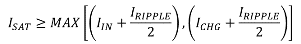
Because the converter might be either operated in the buck mode or the boost mode, so the inductor current is equal to either the charging current or the input current. The inductor saturation current should be higher than the larger value of the input current (IIN) or the charging current (ICHG) plus half the ripple current (IRIPPLE):

Equation 4. GUID-793171D7-59A0-4E96-BE19-912AABD5C441-low.gif

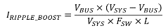
The inductor ripple current (IRIPPLE) depends on the input voltage (VBUS), the output voltage (VSYS), the switching frequency (FSW) and the inductance (L). The inductor current ripples for buck mode and boost mode are calculated with equations (4) and (5), respectively:

Equation 5. GUID-64A5F99D-5DE4-483B-B782-62432766D77F-low.gif
Equation 6. GUID-CD8982F2-44DD-46B5-AFE7-5B42B853DDFC-low.gif

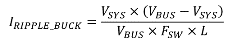
The inductor current ripple in the buck mode is usually larger than that in the boost mode, since the voltage-second applied on the inductor is larger. The maximum inductor current ripple in the buck mode happens in the vicinity of D = VSYS / VBUS = 0.5. The SYS voltage is approximately 8V for the 2s battery configuration, so the worst case for the inductor ripples is with the 15V or 20V input voltage.