SLUSC86D March   2015  – October 2022 BQ25890 , BQ25892

PRODUCTION DATA  

  1. Features
  2. Applications
  3. Description
  4. Revision History
  5. Description (continued)
  6. Device Comparison Table
  7. Pin Configuration and Functions
  8. Specifications
    1. 8.1 Absolute Maximum Ratings (1)
    2. 8.2 ESD Ratings
    3. 8.3 Recommended Operating Conditions
    4. 8.4 Thermal Information
    5. 8.5 Electrical Characteristics
    6. 8.6 Timing Requirements
    7. 8.7 Typical Characteristics
  9. Detailed Description
    1. 9.1 Functional Block Diagram
    2. 9.2 Feature Description
      1. 9.2.1  Device Power-On-Reset (POR)
      2. 9.2.2  Device Power Up from Battery without Input Source
      3. 9.2.3  Device Power Up from Input Source
        1. 9.2.3.1 Power Up REGN Regulation (LDO)
        2. 9.2.3.2 Poor Source Qualification
        3. 9.2.3.3 Input Source Type Detection
          1. 9.2.3.3.1 D+/D– Detection Sets Input Current Limit (BQ25890)
          2. 9.2.3.3.2 PSEL/OTG Pins Set Input Current Limit (BQ25892)
          3. 9.2.3.3.3 Force Input Current Limit Detection
        4. 9.2.3.4 Input Voltage Limit Threshold Setting (VINDPM Threshold)
        5. 9.2.3.5 Converter Power-Up
      4. 9.2.4  Input Current Optimizer (ICO)
      5. 9.2.5  Boost Mode Operation from Battery
      6. 9.2.6  Power Path Management
        1. 9.2.6.1 Narrow VDC Architecture
        2. 9.2.6.2 Dynamic Power Management
        3. 9.2.6.3 Supplement Mode
      7. 9.2.7  Battery Charging Management
        1. 9.2.7.1 Autonomous Charging Cycle
        2. 9.2.7.2 Battery Charging Profile
        3. 9.2.7.3 Charging Termination
        4. 9.2.7.4 Resistance Compensation (IRCOMP)
        5. 9.2.7.5 Thermistor Qualification
          1. 9.2.7.5.1 JEITA Guideline Compliance in Charge Mode
          2. 9.2.7.5.2 Cold/Hot Temperature Window in Boost Mode
        6. 9.2.7.6 Charging Safety Timer
      8. 9.2.8  Battery Monitor
      9. 9.2.9  Status Outputs ( PG, STAT, and INT)
        1. 9.2.9.1 Power Good Indicator ( PG)
        2. 9.2.9.2 Charging Status Indicator (STAT)
        3. 9.2.9.3 Interrupt to Host (INT)
      10. 9.2.10 BATET (Q4) Control
        1. 9.2.10.1 BATFET Disable Mode (Shipping Mode)
        2. 9.2.10.2 BATFET Enable (Exit Shipping Mode)
        3. 9.2.10.3 BATFET Full System Reset
      11. 9.2.11 Current Pulse Control Protocol
      12. 9.2.12 Input Current Limit on ILIM
      13. 9.2.13 Thermal Regulation and Thermal Shutdown
        1. 9.2.13.1 Thermal Protection in Buck Mode
        2. 9.2.13.2 Thermal Protection in Boost Mode
      14. 9.2.14 Voltage and Current Monitoring in Buck and Boost Mode
        1. 9.2.14.1 Voltage and Current Monitoring in Buck Mode
          1. 9.2.14.1.1 Input Overvoltage (ACOV)
          2. 9.2.14.1.2 System Overvoltage Protection (SYSOVP)
        2. 9.2.14.2 Voltage and Current Monitoring in Boost Mode
          1. 9.2.14.2.1 VBUS Overcurrent Protection
          2. 9.2.14.2.2 Boost Mode Overvoltage Protection
      15. 9.2.15 Battery Protection
        1. 9.2.15.1 Battery Overvoltage Protection (BATOVP)
        2. 9.2.15.2 Battery Over-Discharge Protection
        3. 9.2.15.3 System Overcurrent Protection
      16. 9.2.16 Serial Interface
        1. 9.2.16.1 Data Validity
        2. 9.2.16.2 START and STOP Conditions
        3. 9.2.16.3 Byte Format
        4. 9.2.16.4 Acknowledge (ACK) and Not Acknowledge (NACK)
        5. 9.2.16.5 Target Address and Data Direction Bit
        6. 9.2.16.6 Single Read and Write
        7. 9.2.16.7 Multi-Read and Multi-Write
    3. 9.3 Device Functional Modes
      1. 9.3.1 Host Mode and Default Mode
    4. 9.4 Register Maps
      1. 9.4.1  REG00
      2. 9.4.2  REG01
      3. 9.4.3  REG02
      4. 9.4.4  REG03
      5. 9.4.5  REG04
      6. 9.4.6  REG05
      7. 9.4.7  REG06
      8. 9.4.8  REG07
      9. 9.4.9  REG08
      10. 9.4.10 REG09
      11. 9.4.11 REG0A
      12. 9.4.12 REG0B
      13. 9.4.13 REG0C
      14. 9.4.14 REG0D
      15. 9.4.15 REG0E
      16. 9.4.16 REG0F
      17. 9.4.17 REG10
      18. 9.4.18 REG11
      19. 9.4.19 REG12
      20. 9.4.20 REG13
      21. 9.4.21 REG14
  10. 10Application and Implementation
    1. 10.1 Application Information
    2. 10.2 Typical Application
      1. 10.2.1 Design Requirements
      2. 10.2.2 Detailed Design Procedure
        1. 10.2.2.1 Inductor Selection
        2. 10.2.2.2 Buck Input Capacitor
        3. 10.2.2.3 System Output Capacitor
      3. 10.2.3 Application Curves
    3. 10.3 System Examples
  11. 11Power Supply Recommendations
  12. 12Layout
    1. 12.1 Layout Guidelines
    2. 12.2 Layout Example
  13. 13Device and Documentation Support
    1. 13.1 Device Support
      1. 13.1.1 Third-Party Products Disclaimer
    2. 13.2 Receiving Notification of Documentation Updates
    3. 13.3 Support Resources
    4. 13.4 Trademarks
    5. 13.5 Electrostatic Discharge Caution
    6. 13.6 Glossary
  14. 14Mechanical, Packaging, and Orderable Information

Package Options

Mechanical Data (Package|Pins)
Thermal pad, mechanical data (Package|Pins)
Orderable Information
D+/D– Detection Sets Input Current Limit (BQ25890)

The BQ25890 contains a D+/D– based input source detection to set the input current limit automatically. The D+/D- detection includes standard USB BC1.2, non-standard adapter, and adjustable high voltage adapter detections. When input source is plugged-in, the device starts standard USB BC1.2 detections. The USB BC1.2 is capable to identify Standard Downstream Port (SDP), Charging Downstream Port (CDP), and Dedicated Charging Port (DCP). When the Data Contact Detection (DCD) timer of 500ms is expired, the non-standard adapter detection is applied to set the input current limit.

When DCP is detected, the device initates adjustable high voltage adapter handshake including MaxCharge™, etc. The handshake connects combinations of voltage source(s) and/or current sink on D+/D- to signal input source to raise output voltage from 5 V to 9 V / 12 V. The adjustable high voltage adapter handshake can be disabled by clearing MAXC_EN and/or HVDCP_EN bits.
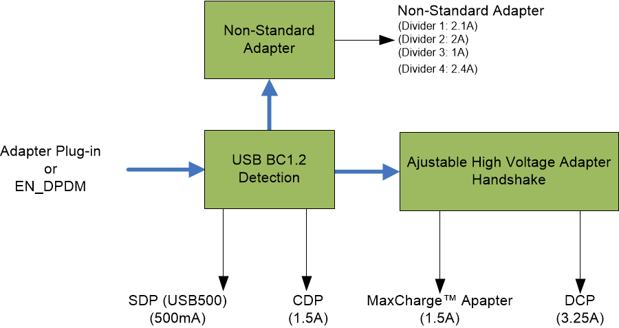
GUID-7037EB33-92C9-4EFD-A1D1-E922F0D4D646-low.gifFigure 9-1 USB D+/D- Detection
Table 9-1 Non-Standard Adapter Detection
NON-STANDARD ADAPTERD+ THRESHOLDD- THRESHOLDINPUT CURRENT LIMIT
Divider 1VD+ within V2P7_VTHVD- within V2P0_VTH2.1A
Divider 2VD+ within V1P2_VTHVD- within V1P2_VTH2A
Divider 3VD+ within V2P0_VTHVD- within V2P7_VTH1A
Divider 4VD+ within V2P7_VTHVD- within V2P7_VTH2.4A
Table 9-2 Adjustable High Voltage Adapter D+/D- Output Configurations
ADJUSTABLE HIGH VOLTAGE HANDSHAKED+D-OUTPUT
MaxCharge (12V)I1P6MA_ISINKV3p45_VSRC12 V
MaxCharge (9V)V3p45_VSRCI1P6MA_ISINK9 V

After the Section 9.2.3.3 is done, an INT pulse is asserted to the host. In addition, the following registers including Input Current Limit register (IINLIM), VBUS_STAT, and SDP_STAT are updated as below:

Table 9-3 BQ25890 Result
D+/D- DETECTIONINPUT CURRENT LIMIT (IINLIM)(1)SDP_STATVBUS_STAT
USB SDP (USB500)500 mA1001
USB CDP1.5 A1010
USB DCP3.25 A1011
Divider 31 A1110
Divider 12.1 A1110
Divider 42.4 A1110
Divider 22 A1110
MaxCharge1.5 A1100
Unknown Adapter500 mA1101
500 mA current limit for 2 min.