SLUSE31A April 2020 – February 2021 BQ25968
PRODUCTION DATA
- 1 Features
- 2 Applications
- 3 Description
- 4 Revision History
- 5 Description (continued)
- 6 Device Comparison Table
- 7 Pin Configuration and Functions
- 8 Specifications
-
9 Detailed Description
- 9.1 Overview
- 9.2 Functional Block Diagram
- 9.3
Feature Description
- 9.3.1 Charging System
- 9.3.2 Battery Charging Profile
- 9.3.3 Control State Diagram for System Implementation
- 9.3.4 Device Power Up
- 9.3.5 Switched Cap Function
- 9.3.6 Charging Start-Up
- 9.3.7 Integrated 16-Bit ADC for Monitoring and Smart Adapter Feedback
- 9.3.8 Device Internal Thermal Shutdown, TSBUS, and TSBAT Temperature Monitoring
- 9.3.9 INT Pin, STAT, FLAG, and MASK Registers
- 9.3.10 CDRVH and CDRVL_ADDRMS Functions
- 9.3.11 Parallel Operation Using Master and Slave Modes
- 9.4 Device Functional Modes
- 9.5 Programming
- 9.6 Register Maps
- 10Application and Implementation
- 11Power Supply Recommendations
- 12Layout
- 13Device and Documentation Support
- 14Mechanical, Packaging, and Orderable Information
Package Options
Mechanical Data (Package|Pins)
- YFF|56
Thermal pad, mechanical data (Package|Pins)
Orderable Information
9.3.2 Battery Charging Profile
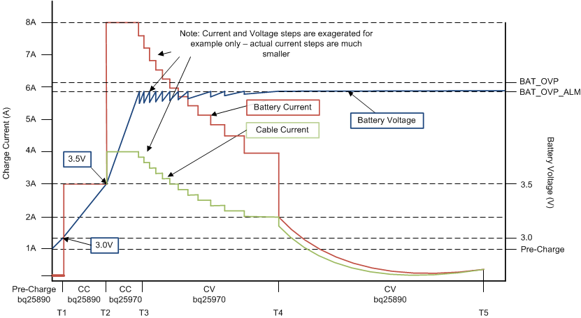
The system will have a specific battery charging profile that is unique due to the switched cap architecture. During the trickle charge and precharge of the battery up to 3.5 V, the charging will be controlled by the primary charger (BQ25890 in Figure 9-1). Once the battery voltage reaches 3.5 V, the adapter can negotiate for a higher bus voltage, enable the BQ25968 charging, and regulate the current on VBUS to charge the battery. In the CC phase, the protection in the BQ25968 will not regulate the battery voltage, but will provide feedback to the system to increase/decrease current as needed, as well as disable the output if the voltage is exceeded. Once the CV point is reached, the BQ25968 will provide feedback to the adapter to reduce the current, effectively tapering the current until a point where the primary charger takes over again. This charging profile is shown in Figure 9-2.
 Figure 9-2 BQ25968 System Charging Profile