SLUSB85E May 2013 – January 2016
PRODUCTION DATA.
- 1 Features
- 2 Applications
- 3 Description
- 4 Revision History
- 5 Device Comparison Table
- 6 Pin Configuration and Functions
-
7 Specifications
- 7.1 Absolute Maximum Ratings
- 7.2 ESD Ratings
- 7.3 Recommended Operating Conditions
- 7.4 Thermal Information
- 7.5 Supply Current
- 7.6 Digital Input and Output DC Characteristics
- 7.7 LDO Regulator, Wake-Up, and Auto-Shutdown DC Characteristics
- 7.8 ADC (Temperature and Cell Measurement) Characteristics
- 7.9 Integrating ADC (Coulomb Counter) Characteristics
- 7.10 Integrated Sense Resistor Characteristics, -40°C to 85°C
- 7.11 Integrated Sense Resistor Characteristics, -40°C to 70°C
- 7.12 I2C-Compatible Interface Communication Timing Characteristics
- 7.13 Typical Characteristics
- 8 Detailed Description
- 9 Applications and Implementation
- 10Power Supply Recommendation
- 11Layout
- 12Device and Documentation Support
- 13Mechanical, Packaging, and Orderable Information
Package Options
Refer to the PDF data sheet for device specific package drawings
Mechanical Data (Package|Pins)
- YZF|9
Thermal pad, mechanical data (Package|Pins)
Orderable Information
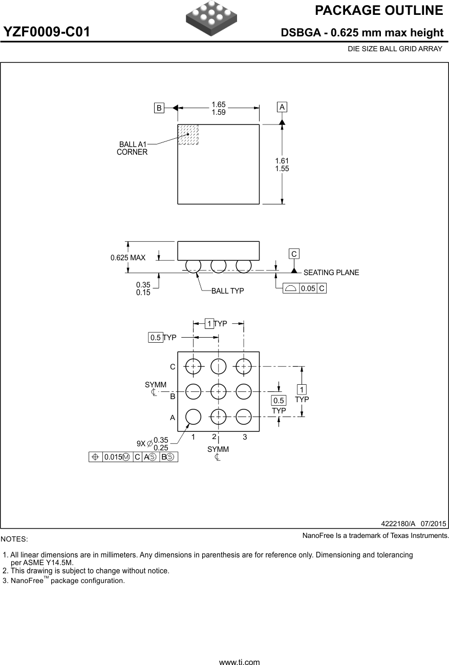
13 Mechanical, Packaging, and Orderable Information
The following pages include mechanical, packaging, and orderable information. This information is the most current data available for the designated devices. This data is subject to change without notice and revision of this document. For browser-based versions of this data sheet, refer to the left-hand navigation.


