SLUSB20C November 2012 – November 2021
PRODUCTION DATA
- 1 Features
- 2 Applications
- 3 Description
- 4 Revision History
- 5 Device Comparison Table
- 6 Pin Configuration and Functions
-
7 Specifications
- 7.1 Absolute Maximum Ratings
- 7.2 ESD Ratings
- 7.3 Recommended Operating Conditions
- 7.4 Thermal Information
- 7.5 Electrical Characteristics: Supply Current
- 7.6 Digital Input and Output DC Characteristics
- 7.7 Power-on Reset
- 7.8 2.5-V LDO Regulator
- 7.9 Internal Clock Oscillators
- 7.10 ADC (Temperature and Cell Measurement) Characteristics
- 7.11 Integrating ADC (Coulomb Counter) Characteristics
- 7.12 Data Flash Memory Characteristics
- 7.13 I2C-Compatible Interface Communication Timing Requirements
- 7.14 Typical Characteristics
- 8 Detailed Description
- 9 Application and Implementation
- 10Power Supply Recommendations
- 11Layout
- 12Device and Documentation Support
- 13Mechanical, Packaging, and Orderable Information
Package Options
Mechanical Data (Package|Pins)
- YZF|15
Thermal pad, mechanical data (Package|Pins)
Orderable Information
8.5.3.1 I2C Interface
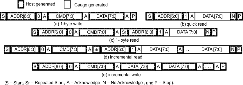
The BQ27520-G4 fuel gauge supports the standard I2C read, incremental read, quick read, one byte write, and incremental write functions. The 7-bit device address (ADDR) is the most significant 7 bits of the hex address and is fixed as 1010101. The first 8-bits of the I2C protocol is, therefore, 0xAA or 0xAB for write or read, respectively.
 Figure 8-3 I2C Read, Incremental Read, Quick Read, One Byte Write, and Incremental Write Functions
The “quick read” returns data at the address indicated by the address pointer. The address pointer, a register internal to the I2C communication engine, increments whenever data is acknowledged by the fuel gauge or the I2C master. “Quick writes” function in the same manner and are a convenient means of sending multiple bytes to consecutive command locations (such as two-byte commands that require two bytes of data).
The following command sequences are not supported:
Attempt to write a read-only address (NACK after data sent by master):
 Figure 8-4 Invalid Write
Attempt to read an address above 0x6B (NACK command):
 Figure 8-5 Invalid Read