SLUS928B March 2009 – July 2016
- 1Features
- 2Applications
- 3Description
- 4Revision History
- 5Pin Configuration and Functions
- 6Specifications
-
7Detailed Description
- 7.1 Feature Description
- 7.2 Device Functional Modes
- 8Device and Documentation Support
- 9Mechanical, Packaging, and Orderable Information
Package Options
Mechanical Data (Package|Pins)
- PW|24
Thermal pad, mechanical data (Package|Pins)
Orderable Information
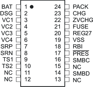
5 Pin Configuration and Functions
PW Package
24-Pin TSSOP
Top View

Pin Functions
| PIN | I/O | DESCRIPTION | |
|---|---|---|---|
| NAME | NO. | ||
| BAT | 1 | P | Power input from battery |
| DSG | 2 | O | P-CH FET Drive controlling discharge |
| VC1 | 3 | IA | Sense voltage input terminal and external cell balancing drive output for most positive cell, and battery stack measurement input. |
| VC2 | 4 | IA | Sense voltage input terminal and external cell balancing drive output for second most positive cell. |
| VC3 | 5 | IA | Sense voltage input terminal and external cell balancing drive output for third most positive cell. |
| VC4 | 6 | IA | Sense voltage input terminal and external cell balancing drive output for least positive cell. |
| SRP | 7 | IA | Analog input pin connected to the internal coulomb-counter peripheral for integrating a small voltage between SRP and SRN where SRP is the top of the sense resistor. |
| SRN | 8 | IA | Analog input pin connected to the internal coulomb-counter peripheral for integrating a small voltage between SRP and SRN where SRN is the bottom of the sense resistor. |
| TS1 | 9 | I/O,IA | Thermistor input TS1 |
| TS2 | 10 | I/O,IA | Thermistor input TS2 |
| NC | 11 | — | Keep this pin floating |
| NC | 12 | — | Keep this pin floating |
| NC | 13 | — | Keep this pin floating |
| SMBD | 14 | I/OD | SMBus data pin |
| NC | 15 | — | Keep this pin floating |
| SMBC | 16 | I/OD | SMBus clock pin |
| PRES | 17 | I/OD | Active low input to sense system insertion and typically requires additional ESD protection |
| RBI | 18 | P | RAM backup pin to provide backup potential to the internal DATA RAM if power is momentarily lost by using a capacitor attached between RBI and VSS |
| VSS | 19 | P | Device ground |
| REG27 | 20 | P | Internal power supply 2.7V bias output |
| FUSE | 21 | I/OD | Push-pull fuse drive and secondary protector activation input sensing |
| ZVCHG | 22 | O | P-CH precharge FET Drive controlling pre-charge and zero-volt charge |
| CHG | 23 | O | P-CH FET Drive controlling charge |
| PACK | 24 | P | PACK positive terminal and alternative power source |