SLUSC16B November 2015 – March 2019
PRODUCTION DATA.
- 1 Features
- 2 Applications
- 3 Description
- 4 Revision History
- 5 Pin Configuration and Functions
- 6 Specifications
- 7 Detailed Description
- 8 Application and Implementation
- 9 Power Supply Recommendations
- 10Layout
- 11Device and Documentation Support
- 12Mechanical, Packaging, and Orderable Information
Package Options
Mechanical Data (Package|Pins)
- PW|16
Thermal pad, mechanical data (Package|Pins)
Orderable Information
8.1.1.4 Precharge and Predischarge Support
For a deeply depleted battery pack, a much lower charging current, for example, a C/10 rate, is usually used to precharge the battery cells. This allows the passivating layer of the cell to be recovered slowly (the passivating layer might be dissolved in the deep discharge state).
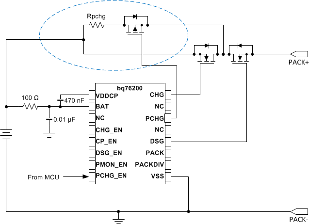
The bq76200 has a PCHG output to drive an external P-channel FET to support battery precharge. In this scenario, the external P-channel FET is placed in parallel with the CHG FET and a power resistor can be connected in series of the P-channel FET to limit the charging current during the precharge state. The MCU can be used to control the PCHG_EN pin to determine the entry and exit of the precharge mode.
 Figure 9. P-Channel FET in Parallel with CHG FET for Precharging (Partial Schematic Shown)
 Alternatively, the CHG pin can also be used to precharge a battery pack given if the charging current is controlled by the system (that is, does not require external component to limit the charging current such as a smart charger) and the battery stack voltage is higher than minimum operation voltage of the bq76200 (that is, the charge pump can start to turn on the CHG FET). PCHG should leave floating if it is not used in the application.
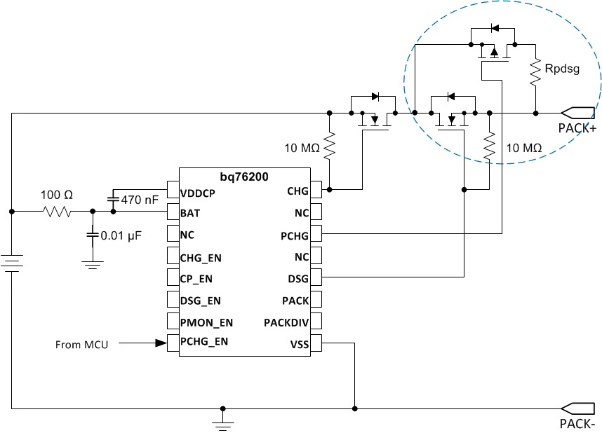
The PCHG output can be used to predischarge a high-capacitive system. For example, a load removal can be one of the recovery requirements after a discharge related fault has been detected. In a high-capacitive system, the residual voltage at the system side can take a significant time to bleed off. This results in an additional delay in fault recovery. The PCHG output can be used to control an external P-channel FET placed in parallel with the DSG FET to predischarge the residual voltage in order to speed up the fault recovery process.
 Figure 10. P-Channel FET in Parallel with DSG FET for Predischarging (Partial Schematic Shown)