SLUSBK2I October 2013 – March 2022 BQ76920 , BQ76930 , BQ76940
PRODMIX
- 1 Features
- 2 Applications
- 3 Description
- 4 Revision History
- 5 Device Comparison Table
- 6 Pin Configuration and Functions
- 7 Specifications
- 8 Detailed Description
- 9 Application and Implementation
- 10Power Supply Recommendations
- 11Layout
- 12Device and Documentation Support
- 13Mechanical, Packaging, and Orderable Information
Package Options
Mechanical Data (Package|Pins)
- DBT|30
Thermal pad, mechanical data (Package|Pins)
Orderable Information
6.3 BQ76930 Pin Diagram
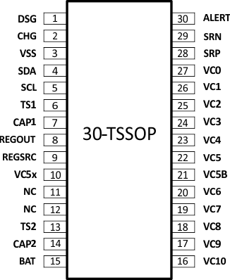
Table 6-2 BQ76930 Pin Functions
| PIN | NAME | TYPE | DESCRIPTION |
|---|---|---|---|
| 1 | DSG | O | Discharge FET driver |
| 2 | CHG | O | Charge FET driver |
| 3 | VSS | — | Chip VSS |
| 4 | SDA | I/O | I2C communication to the host controller |
| 5 | SCL | I | I2C communication to the host controller |
| 6 | TS1 | I | Thermistor #1 positive terminal(1) |
| 7 | CAP1 | O | Capacitor to VSS |
| 8 | REGOUT | P | Output LDO |
| 9 | REGSRC | I | Input source for output LDO |
| 10 | VC5X | P | Thermistor #2 negative terminal |
| 11 | NC | — | No connect (short to CAP2) |
| 12 | NC | — | No connect (short to CAP2) |
| 13 | TS2 | I | Thermistor #2 positive terminal(1) |
| 14 | CAP2 | O | Capacitor to VC5X |
| 15 | BAT | P | Battery (top-most) terminal |
| 16 | VC10 | I | Sense voltage for 10th cell positive terminal |
| 17 | VC9 | I | Sense voltage for 9th cell positive terminal |
| 18 | VC8 | I | Sense voltage for 8th cell positive terminal |
| 19 | VC7 | I | Sense voltage for 7th cell positive terminal |
| 20 | VC6 | I | Sense voltage for 6th cell positive terminal |
| 21 | VC5B | I | Sense voltage for 6th cell negative terminal |
| 22 | VC5 | I | Sense voltage for 5th cell positive terminal |
| 23 | VC4 | I | Sense voltage for 4th cell positive terminal |
| 24 | VC3 | I | Sense voltage for 3rd cell positive terminal |
| 25 | VC2 | I | Sense voltage for 2nd cell positive terminal |
| 26 | VC1 | I | Sense voltage for 1st cell positive terminal |
| 27 | VC0 | I | Sense voltage for 1st cell negative terminal |
| 28 | SRP | I | Negative current sense (nearest VSS) |
| 29 | SRN | I | Positive current sense |
| 30 | ALERT | I/O | Alert output and override input |
(1) If not used, pull down to group ground reference (VSS for TS1
and VC5X for TS2) with a 10-kΩ nominal resistor.