SLUSBK2I October   2013  – March 2022 BQ76920 , BQ76930 , BQ76940

PRODMIX  

  1. Features
  2. Applications
  3. Description
  4. Revision History
  5. Device Comparison Table
  6. Pin Configuration and Functions
    1. 6.1 Versions
    2. 6.2 BQ76920 Pin Diagram
    3. 6.3 BQ76930 Pin Diagram
    4. 6.4 BQ76940 Pin Diagram
  7. Specifications
    1. 7.1 Absolute Maximum Ratings
    2. 7.2 ESD Ratings
    3. 7.3 Recommended Operating Conditions
    4. 7.4 Thermal Information
    5. 7.5 Electrical Characteristics
    6. 7.6 Timing Requirements
    7. 7.7 Typical Characteristics
  8. Detailed Description
    1. 8.1 Overview
    2. 8.2 Functional Block Diagram
    3. 8.3 Feature Description
      1. 8.3.1 Subsystems
        1. 8.3.1.1 Measurement Subsystem Overview
          1. 8.3.1.1.1 Data Transfer to the Host Controller
          2. 8.3.1.1.2 14-Bit ADC
            1. 8.3.1.1.2.1 Optional Real-Time Calibration Using the Host Microcontroller
          3. 8.3.1.1.3 16-Bit CC
          4. 8.3.1.1.4 External Thermistor
          5. 8.3.1.1.5 Die Temperature Monitor
          6. 8.3.1.1.6 16-Bit Pack Voltage
          7. 8.3.1.1.7 System Scheduler
        2. 8.3.1.2 Protection Subsystem
          1. 8.3.1.2.1 Integrated Hardware Protections
          2. 8.3.1.2.2 Reduced Test Time
        3. 8.3.1.3 Control Subsystem
          1. 8.3.1.3.1 FET Driving (CHG AND DSG)
            1. 8.3.1.3.1.1 High-Side FET Driving
          2. 8.3.1.3.2 Load Detection
          3. 8.3.1.3.3 Cell Balancing
          4. 8.3.1.3.4 Alert
          5. 8.3.1.3.5 Output LDO
        4. 8.3.1.4 Communications Subsystem
    4. 8.4 Device Functional Modes
      1. 8.4.1 NORMAL Mode
      2. 8.4.2 SHIP Mode
    5. 8.5 Register Maps
      1. 8.5.1 Register Details
      2. 8.5.2 Read-Only Registers
  9. Application and Implementation
    1. 9.1 Application Information
      1. 9.1.1 Device Timing
      2. 9.1.2 Random Cell Connection
      3. 9.1.3 Power Pin Diodes
      4. 9.1.4 Alert Pin
      5. 9.1.5 Sense Inputs
      6. 9.1.6 TSn Pins
      7. 9.1.7 Unused Pins
      8. 9.1.8 Configuring Alternative Cell Counts
    2. 9.2 Typical Applications
      1. 9.2.1 Design Requirements
      2. 9.2.2 Detailed Design Procedure
        1. 9.2.2.1 Step-by-Step Design Procedure
      3. 9.2.3 Application Curves
  10. 10Power Supply Recommendations
  11. 11Layout
    1. 11.1 Layout Guidelines
    2. 11.2 Layout Example
  12. 12Device and Documentation Support
    1. 12.1 Third-Party Products Disclaimer
    2. 12.2 Documentation Support
    3. 12.3 Related Links
    4. 12.4 Receiving Notification of Documentation Updates
    5. 12.5 Trademarks
  13. 13Mechanical, Packaging, and Orderable Information

Package Options

Mechanical Data (Package|Pins)
Thermal pad, mechanical data (Package|Pins)
Orderable Information
FET Driving (CHG AND DSG)

Each BQ769x0 device provides two low-side FET drivers, CHG and DSG, which control NCH power FETs or may be used as a signal to enable various other circuits such as a high-side NCH charge pump circuit.

Both DSG and CHG drivers have a fast pull-up to nominally 12 V when enabled. DSG uses a fast pull-down to VSS when disabled, while CHG utilizes a high impedance (nominally 1 MΩ) pull-down path when disabled.

An additional internal clamp circuit ensures that the CHG pin does not exceed a maximum of 20 V.
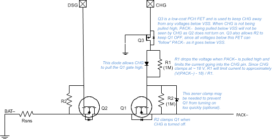
GUID-A00F2962-CD5B-4DBD-9FB6-AF54A2CADC8F-low.gifFigure 8-2 CHG and DSG FET Circuit

The power path for the CHG and DSG pull-up circuit originates from the REGSRC pin, instead of BAT.

To enable the CHG fet, set the [CHG_ON] register bit to 1; to disable, set [CHG_ON] = 0. The discharge FET may be similarly controlled through the [DSG_ON] register bit.

Certain fault conditions or power state transitions will clear the state of the CHG/DSG FET controls. Table 8-1 shows what action, if any, to take to [CHG_ON] and [DSG_ON] in response to various system events: