SLUSBK2I October   2013  – March 2022 BQ76920 , BQ76930 , BQ76940

PRODMIX  

  1. Features
  2. Applications
  3. Description
  4. Revision History
  5. Device Comparison Table
  6. Pin Configuration and Functions
    1. 6.1 Versions
    2. 6.2 BQ76920 Pin Diagram
    3. 6.3 BQ76930 Pin Diagram
    4. 6.4 BQ76940 Pin Diagram
  7. Specifications
    1. 7.1 Absolute Maximum Ratings
    2. 7.2 ESD Ratings
    3. 7.3 Recommended Operating Conditions
    4. 7.4 Thermal Information
    5. 7.5 Electrical Characteristics
    6. 7.6 Timing Requirements
    7. 7.7 Typical Characteristics
  8. Detailed Description
    1. 8.1 Overview
    2. 8.2 Functional Block Diagram
    3. 8.3 Feature Description
      1. 8.3.1 Subsystems
        1. 8.3.1.1 Measurement Subsystem Overview
          1. 8.3.1.1.1 Data Transfer to the Host Controller
          2. 8.3.1.1.2 14-Bit ADC
            1. 8.3.1.1.2.1 Optional Real-Time Calibration Using the Host Microcontroller
          3. 8.3.1.1.3 16-Bit CC
          4. 8.3.1.1.4 External Thermistor
          5. 8.3.1.1.5 Die Temperature Monitor
          6. 8.3.1.1.6 16-Bit Pack Voltage
          7. 8.3.1.1.7 System Scheduler
        2. 8.3.1.2 Protection Subsystem
          1. 8.3.1.2.1 Integrated Hardware Protections
          2. 8.3.1.2.2 Reduced Test Time
        3. 8.3.1.3 Control Subsystem
          1. 8.3.1.3.1 FET Driving (CHG AND DSG)
            1. 8.3.1.3.1.1 High-Side FET Driving
          2. 8.3.1.3.2 Load Detection
          3. 8.3.1.3.3 Cell Balancing
          4. 8.3.1.3.4 Alert
          5. 8.3.1.3.5 Output LDO
        4. 8.3.1.4 Communications Subsystem
    4. 8.4 Device Functional Modes
      1. 8.4.1 NORMAL Mode
      2. 8.4.2 SHIP Mode
    5. 8.5 Register Maps
      1. 8.5.1 Register Details
      2. 8.5.2 Read-Only Registers
  9. Application and Implementation
    1. 9.1 Application Information
      1. 9.1.1 Device Timing
      2. 9.1.2 Random Cell Connection
      3. 9.1.3 Power Pin Diodes
      4. 9.1.4 Alert Pin
      5. 9.1.5 Sense Inputs
      6. 9.1.6 TSn Pins
      7. 9.1.7 Unused Pins
      8. 9.1.8 Configuring Alternative Cell Counts
    2. 9.2 Typical Applications
      1. 9.2.1 Design Requirements
      2. 9.2.2 Detailed Design Procedure
        1. 9.2.2.1 Step-by-Step Design Procedure
      3. 9.2.3 Application Curves
  10. 10Power Supply Recommendations
  11. 11Layout
    1. 11.1 Layout Guidelines
    2. 11.2 Layout Example
  12. 12Device and Documentation Support
    1. 12.1 Third-Party Products Disclaimer
    2. 12.2 Documentation Support
    3. 12.3 Related Links
    4. 12.4 Receiving Notification of Documentation Updates
    5. 12.5 Trademarks
  13. 13Mechanical, Packaging, and Orderable Information

Package Options

Mechanical Data (Package|Pins)
Thermal pad, mechanical data (Package|Pins)
Orderable Information

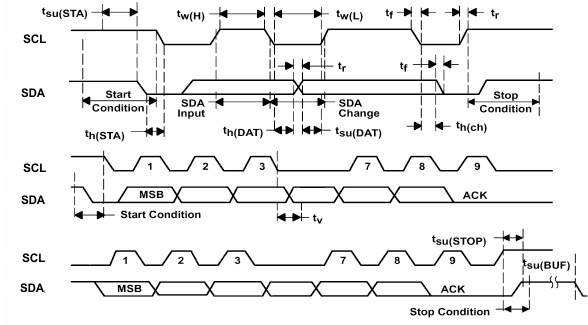
Timing Requirements

I2C COMPATIBLE INTERFACEMINTYPMAXUNIT
VILInput low logic thresholdREGOUT x 0.25V
VIHInput high logic thresholdREGOUT x 0.75V
VOLOutput low logic drive0.20V
tfSCL, SDA fall time0.40
VOHOutput high logic drive (not applicable due to open-drain outputs)N/AN/AV
tHIGHSCL pulse width high4.0µs
tLOWSCL pulse width low4.7µs
tSU;STASetup time for START condition4.7µs
tHD;STASTART condition hold time after which first clock pulse is generated4.0µs
tSU;DATData setup time250ns
tHD;DATData hold time0µs
tSU;STOSetup time for STOP condition4.0µs
tBUFTime the bus must be free before new transmission can start4.7µs
tVD;DATClock low to data out valid900ns
tHD;DATData out hold time after clock low0ns
fSCLClock frequency0100kHz
GUID-D2189E3E-2A03-4012-9559-E61203D46D03-low.gifFigure 7-1 I2C Timing