SLUSE14B December 2020 – December 2021 BQ76942
PRODUCTION DATA
- 1 Features
- 2 Applications
- 3 Description
- 4 Revision History
- 5 Device Comparison Table
- 6 Pin Configuration and Functions
-
7 Specifications
- 7.1 Absolute Maximum Ratings
- 7.2 ESD Ratings
- 7.3 Recommended Operating Conditions
- 7.4 Thermal Information BQ76942
- 7.5 Supply Current
- 7.6 Digital I/O
- 7.7 LD Pin
- 7.8 Precharge (PCHG) and Predischarge (PDSG) FET Drive
- 7.9 FUSE Pin Functionality
- 7.10 REG18 LDO
- 7.11 REG0 Pre-regulator
- 7.12 REG1 LDO
- 7.13 REG2 LDO
- 7.14 Voltage References
- 7.15 Coulomb Counter
- 7.16 Coulomb Counter Digital Filter (CC1)
- 7.17 Current Measurement Digital Filter (CC2)
- 7.18 Current Wake Detector
- 7.19 Analog-to-Digital Converter
- 7.20 Cell Balancing
- 7.21 Cell Open Wire Detector
- 7.22 Internal Temperature Sensor
- 7.23 Thermistor Measurement
- 7.24 Internal Oscillators
- 7.25 High-Side NFET Drivers
- 7.26 Comparator-Based Protection Subsystem
- 7.27 Timing Requirements – I2C Interface, 100kHz Mode
- 7.28 Timing Requirements – I2C Interface, 400kHz Mode
- 7.29 Timing Requirements – HDQ Interface
- 7.30 Timing Requirements – SPI Interface
- 7.31 Interface Timing Diagrams
- 7.32 Typical Characteristics
- 8 Device Description
- 9 Device Configuration
-
10Measurement Subsystem
- 10.1 Voltage Measurement
- 10.2 General Purpose ADCIN Functionality
- 10.3 Coulomb Counter and Digital Filters
- 10.4 Synchronized Voltage and Current Measurement
- 10.5 Internal Temperature Measurement
- 10.6 Thermistor Temperature Measurement
- 10.7 Factory Trim of Voltage ADC
- 10.8 Voltage Calibration (ADC Measurements)
- 10.9 Voltage Calibration (COV and CUV Protections)
- 10.10 Current Calibration
- 10.11 Temperature Calibration
- 11Primary and Secondary Protection Subsystems
-
12Device Hardware Features
- 12.1 Voltage References
- 12.2 ADC Multiplexer
- 12.3 LDOs
- 12.4 Standalone Versus Host Interface
- 12.5 Multifunction Pin Controls
- 12.6 RST_SHUT Pin Operation
- 12.7 CFETOFF, DFETOFF, BOTHOFF Pin Functionality
- 12.8 ALERT Pin Operation
- 12.9 DDSG and DCHG Pin Operation
- 12.10 Fuse Drive
- 12.11 Cell Open Wire
- 12.12 Low Frequency Oscillator
- 12.13 High Frequency Oscillator
- 13Device Functional Modes
- 14Serial Communications Interface
- 15Cell Balancing
- 16Application and Implementation
- 17Power Supply Requirements
- 18Layout
- 19Device and Documentation Support
- 20Mechanical, Packaging, Orderable Information
Package Options
Mechanical Data (Package|Pins)
- PFB|48
Thermal pad, mechanical data (Package|Pins)
- PFB|48
Orderable Information
7.32 Typical Characteristics
Figure 7-4 Cell
Voltage Measurement Error at 25°C Across Input Range
Figure 7-6 Cell
Voltage Measurement Error vs. Temperature with Cell Voltage = 2.5 V
Figure 7-8 Cell
Voltage Measurement Error vs. Temperature with Cell Voltage = 4.5 V
Error in
measurement of differential voltage between SRP and SRN pins.
Figure 7-10 Current Measurement Error vs. TemperatureFigure 7-12 Internal Temperature Sensor
(Delta VBE)
Voltage vs. Temperature
Figure 7-14 High
Frequency Oscillator (HFO) Accuracy vs. Temperature
Figure 7-16 Overcurrent in Charge Protection (OCC) Threshold vs. Temperature
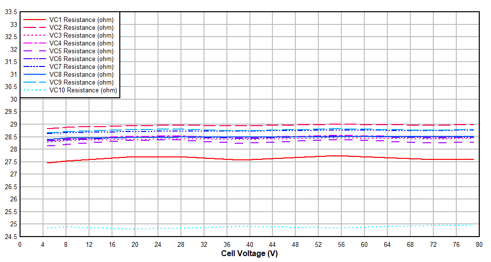
This test uses a resistor divider across the VCx pins to enable one common voltage to be scaled across the cell inputs. The top of the string is swept and captured as the cell voltage.
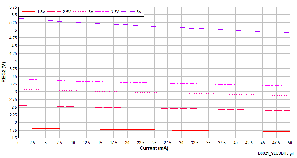 Figure 7-20 REG2
Voltage vs. Load at 25°C
Figure 7-20 REG2
Voltage vs. Load at 25°CFigure 7-22 Thermistor Pullup Resistance vs. Temperature
(180-kΩ
Setting)
Figure 7-24 LD
Wake Voltage vs. Temperature
Figure 7-26 REG18
Voltage vs. Temperature, across BAT Levels
Figure 7-28 BAT
Current in NORMAL Mode vs. Temperature
Figure 7-30 BAT
Current in SLEEP2 (SRC Follower) Mode vs. Temperature
Figure 7-5 Cell
Voltage Measurement Error vs. Temperature with Cell Voltage = 1.5 V
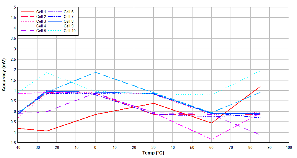 Figure 7-7 Cell
Voltage Measurement Error vs. Temperature with Cell Voltage = 3.5 V
Figure 7-7 Cell
Voltage Measurement Error vs. Temperature with Cell Voltage = 3.5 VFigure 7-9 Cell
Voltage Measurement Error vs. Temperature with Cell Voltage = 5.5 V
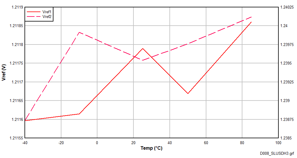 Figure 7-11 Internal Voltage References vs. Temperature
(VREF1
and
VREF2)
Figure 7-11 Internal Voltage References vs. Temperature
(VREF1
and
VREF2)LFO
measured in full speed mode (262 kHz)
Figure 7-13 Low
Frequency Oscillator (LFO) Accuracy vs. Temperature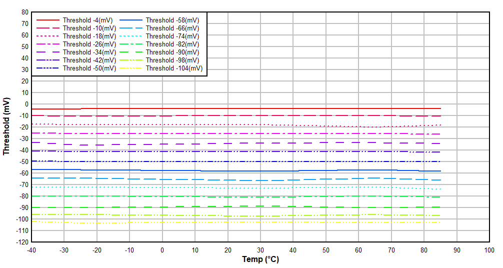 Figure 7-15 Overcurrent in Discharge Protection 1 (OCD1) Threshold vs.
Temperature
Figure 7-15 Overcurrent in Discharge Protection 1 (OCD1) Threshold vs.
TemperatureFigure 7-17 Cell
Balancing Resistance vs. Temperature
Figure 7-19 REG1
Voltage vs. Load at 25°C
Figure 7-21 Thermistor Pullup Resistance vs. Temperature
(18-kΩ
Setting)
Error calculated as percentage
of nominal gain across
±200-mV
input range
Figure 7-23 Coulomb Counter Gain Error vs. Temperature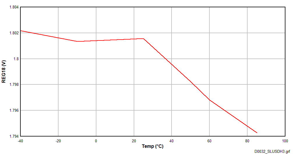 Figure 7-25 REG18
Voltage vs. Temperature, with No Load
Figure 7-25 REG18
Voltage vs. Temperature, with No LoadMeasurements taken using
external BJT
Figure 7-27 REGIN
Voltage vs. BAT Voltage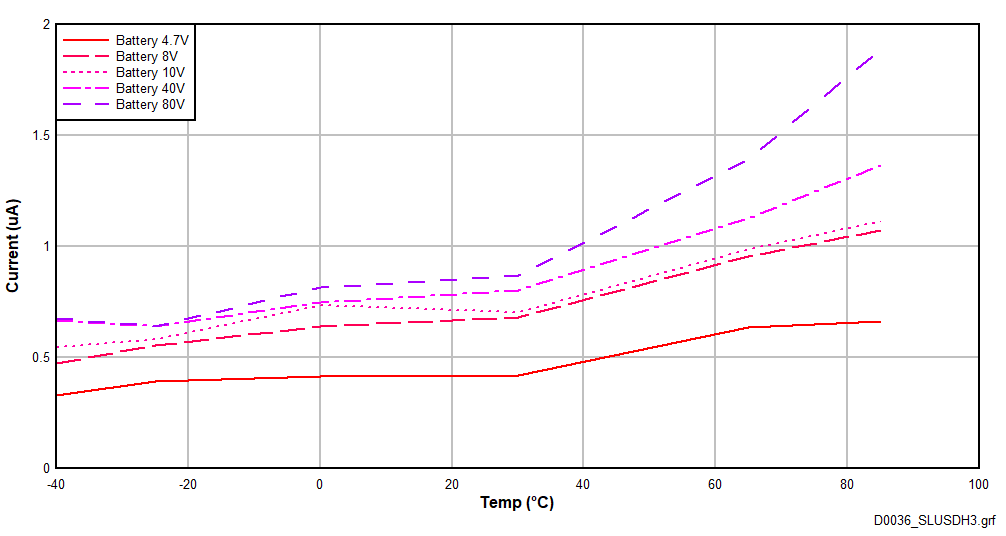 Figure 7-29 BAT
Current in SHUTDOWN Mode vs. Temperature
Figure 7-29 BAT
Current in SHUTDOWN Mode vs. TemperatureFigure 7-31 BAT
Current in DEEPSLEEP2 (No LFO) Mode vs. Temperature