SLUSAX1L December 2012 – June 2021 BQ7718
PRODMIX
- 1 Features
- 2 Applications
- 3 Description
- 4 Revision History
- 5 Device Comparison Table
- 6 Pin Configuration and Functions
- 7 Specifications
- 8 Detailed Description
- 9 Application and Implementation
- 10Power Supply Recommendations
- 11Layout
- 12Device and Documentation Support
- 13Mechanical, Packaging, and Orderable Information
Package Options
Mechanical Data (Package|Pins)
- DPJ|8
Thermal pad, mechanical data (Package|Pins)
Orderable Information
8.4.3 Customer Test Mode
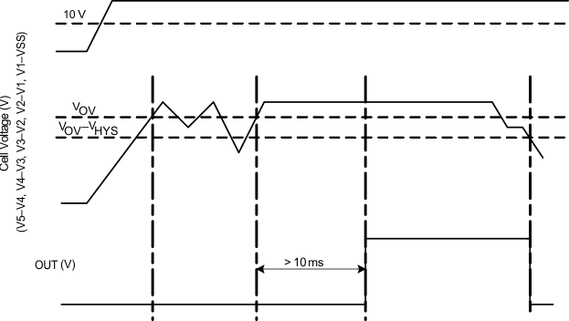
Customer Test Mode (CTM) helps to reduce test time for checking the overvoltage delay timer parameter once the circuit is implemented in the battery pack. To enter CTM, VDD should be set to at least 10 V higher than V5 (see Figure 8-2). The delay timer is greater than 10 ms, but considerably shorter than the timer delay in normal operation. To exit Customer Test Mode, remove the VDD to a V5 voltage differential of 10 V so that the decrease in this value automatically causes an exit.
Avoid exceeding any Absolute Maximum Voltages on any pins when placing the part into Customer Test Mode. Also avoid exceeding Absolute Maximum Voltages for the individual cell voltages (V5–V4), (V4–V3), (V4–V3), (V3–V2), (V2–V1), and (V1–VSS). Stressing the pins beyond the rated limits may cause permanent damage to the device.
Figure 8-2 shows the timing for the Customer Test Mode.
 Figure 8-2 Timing for Customer Test Mode