SLUSCM3K June 2016 – July 2020 BQ77904 , BQ77905
PRODUCTION DATA
- 1 Features
- 2 Applications
- 3 Description
- 4 Revision History
- 5 Device Comparison
- 6 Pin Configuration and Functions
- 7 Specifications
-
8 Detailed Description
- 8.1 Overview
- 8.2 Functional Block Diagram
- 8.3
Feature Description
- 8.3.1 Protection Summary
- 8.3.2
Fault Operation
- 8.3.2.1 Operation in OV
- 8.3.2.2 Operation in UV
- 8.3.2.3 Operation in OW
- 8.3.2.4 Operation in OCD1
- 8.3.2.5 Operation in OCD2
- 8.3.2.6 Operation in SCD
- 8.3.2.7 Overcurrent Recovery Timer
- 8.3.2.8 Load Removal Detection
- 8.3.2.9 Load Removal Detection in UV
- 8.3.2.10 Operation in OTC
- 8.3.2.11 Operation in OTD
- 8.3.2.12 Operation in UTC
- 8.3.2.13 Operation in UTD
- 8.3.3 Protection Response and Recovery Summary
- 8.3.4 Configuration CRC Check and Comparator Built-In-Self-Test
- 8.3.5 Fault Detection Method
- 8.3.6 State Comparator
- 8.3.7 DSG FET Driver Operation
- 8.3.8 CHG FET Driver Operation
- 8.3.9 External Override of CHG and DSG Drivers
- 8.3.10 Configuring 3-S, 4-S, or 5-S Mode
- 8.3.11 Stacking Implementations
- 8.3.12 Zero-Volt Battery Charging Inhibition
- 8.4 Device Functional Modes
- 9 Application and Implementation
- 10Power Supply Recommendations
- 11Layout
- 12Device and Documentation Support
- 13Mechanical, Packaging, and Orderable Information
Package Options
Mechanical Data (Package|Pins)
- PW|20
Thermal pad, mechanical data (Package|Pins)
- PW|20
Orderable Information
8.3.8 CHG FET Driver Operation
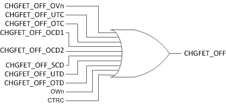
The CHG and CHGU pins are driven high only when no related faults (OV, OW, OTC, UTC, OTD, UTD, OCD1, OCD2, SCD, and CTRC are disabled) are present or the pack has a discharge current where (SRP-SRN) < VSTATE_D1 . The CHG pin drives the CHG FET, which is for use on the single device configuration or by the bottom device in a stack configuration. The CHGU pin has the same logic state as the CHG pin and is for use in the upper device (in a multi-stack configuration) to provide the drive signal to the CTRC pin of the lower device. The CHGU pin should never connect to the CHG FET directly.
Turning off the CHG pin has no influence on the overcurrent protection circuitry. The CHG pin is designed to switch on quickly and the target on resistance is about 2 kΩ. When the pin is turned off, the CHG driver pin is actively driven low and will fall together with PACK–.
The CHG FET may be turned on to protect the FET's body diode if the pack is discharging, even if a charging inhibit fault condition is present. This is done through the state comparator. The state comparator (with the VSTATE_D threshold) remains on for the entire duration of a DSG fault with no CHG fault event.
- If (SRP-SRN) > VSTATE_D and no discharge event is detected, the CHG FET output will remain OFF due to the present of a CHG fault.
- If (SRP-SRN) ≤ VSTATE_D and a charge event is detected, the CHG FET output will turn ON for body diode protection.
The CHGFET_OFF signal is a result of the presence of any related faults, as shown in Figure 8-7.
 Figure 8-7 Faults That Can Qualify CHGFET OFF