SLUSCU0L march 2018 – august 2023 BQ77915
PRODUCTION DATA
- 1
- 1 Features
- 2 Applications
- 3 Description
- 4 Revision History
- 5 Description (continued)
- 6 Device Comparison Table
- 7 Pin Configuration and Functions
- 8 Specifications
-
9 Detailed Description
- 9.1 Overview
- 9.2 Functional Block Diagram
- 9.3
Feature Description
- 9.3.1 Protection Summary
- 9.3.2
Fault Operation
- 9.3.2.1 Operation in OV
- 9.3.2.2 Operation in UV
- 9.3.2.3 Operation in OW
- 9.3.2.4 Operation in OCD1
- 9.3.2.5 Operation in OCD2
- 9.3.2.6 Programming the OCD1/2 Delay Using the OCDP Pin
- 9.3.2.7 Operation in SCD
- 9.3.2.8 Operation in OCC
- 9.3.2.9 Overcurrent Recovery Timer
- 9.3.2.10 Load Detection and Load Removal Detection
- 9.3.2.11 Operation in OTC
- 9.3.2.12 Operation in OTD
- 9.3.2.13 Operation in UTC
- 9.3.2.14 Operation in UTD
- 9.3.3 Protection Response and Recovery Summary
- 9.3.4 Cell Balancing
- 9.3.5 HIBERNATE Mode Operation
- 9.3.6 Configuration CRC Check and Comparator Built-In-Self-Test
- 9.3.7 Fault Detection Method
- 9.3.8 State Comparator
- 9.3.9 DSG FET Driver Operation
- 9.3.10 CHG FET Driver Operation
- 9.3.11 External Override of CHG and DSG Drivers
- 9.3.12 Configuring 3-Series, 4-Series, or 5-Series Modes
- 9.3.13 Stacking Implementations
- 9.3.14 Zero-Volt Battery Charging Inhibition
- 9.4 Device Functional Modes
-
10Application and Implementation
- 10.1
Application Information
- 10.1.1 Recommended System Implementation
- 10.2 Typical Application
- 10.1
Application Information
- 11Power Supply Recommendations
- 12Layout
- 13Device and Documentation Support
- 14Mechanical, Packaging, and Orderable Information
Package Options
Mechanical Data (Package|Pins)
- PW|24
Thermal pad, mechanical data (Package|Pins)
Orderable Information
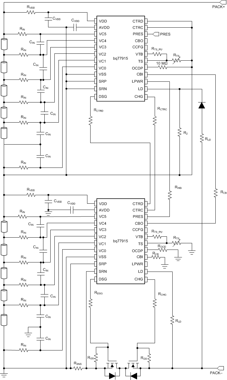
9.3.13 Stacking Implementations
To support higher than 5-series cell packs, daisy-chain multiple devices. Each device has OV, UV, OW, OTC, OTD, UTC, and UTD protections of its directly monitored cells, while any fault conditions disable the global CHG and/or DSG FET driver automatically.
Upper devices do not provide OCC, OCD1, OCD2, or SCD protections, as these are based on pack current. For the BQ77915 device used on the upper stack, short the SRP and SRN pins to prevent false detection.
To configure higher-cell packs, follow this procedure:
- Connect each device on at least each of its three lowest cell input pins.
- Connect a higher cell count to the upper devices (for example, for a 7-series configuration, connect four cells on the upper device and three cells on the bottom device). This provides a stronger CTRx signal to the bottom device.
- Verify each device’s CCFG pin is configured appropriately for its specific number of cells (that is, three, four, or five cells).
- Connect the upper CHG pins with an RCTRx to the immediate lower device CTRC pin.
- Connect the upper DSG pins with an RCTRx to the immediate lower device CTRD pin.
- All upper devices should have their SRP and SRN pins shorted to their VSS pins.
- Connect the upper CBI pins with an RCB to the immediate lower device CBO pin.
- Connect the upper LPWR pins with an RHIB to the immediate lower device PRES pin.
- Connect the upper OCDP pins with a 10-MΩ resistor to VSS. Use the lower OCDP pin to program the OCD1/2 delay.
 Figure 9-14 10-Series Configuration with Internal Cell Balancing and HIBERNATE Mode Enabled