SLUSCU0L march 2018 – august 2023 BQ77915
PRODUCTION DATA
- 1
- 1 Features
- 2 Applications
- 3 Description
- 4 Revision History
- 5 Description (continued)
- 6 Device Comparison Table
- 7 Pin Configuration and Functions
- 8 Specifications
-
9 Detailed Description
- 9.1 Overview
- 9.2 Functional Block Diagram
- 9.3
Feature Description
- 9.3.1 Protection Summary
- 9.3.2
Fault Operation
- 9.3.2.1 Operation in OV
- 9.3.2.2 Operation in UV
- 9.3.2.3 Operation in OW
- 9.3.2.4 Operation in OCD1
- 9.3.2.5 Operation in OCD2
- 9.3.2.6 Programming the OCD1/2 Delay Using the OCDP Pin
- 9.3.2.7 Operation in SCD
- 9.3.2.8 Operation in OCC
- 9.3.2.9 Overcurrent Recovery Timer
- 9.3.2.10 Load Detection and Load Removal Detection
- 9.3.2.11 Operation in OTC
- 9.3.2.12 Operation in OTD
- 9.3.2.13 Operation in UTC
- 9.3.2.14 Operation in UTD
- 9.3.3 Protection Response and Recovery Summary
- 9.3.4 Cell Balancing
- 9.3.5 HIBERNATE Mode Operation
- 9.3.6 Configuration CRC Check and Comparator Built-In-Self-Test
- 9.3.7 Fault Detection Method
- 9.3.8 State Comparator
- 9.3.9 DSG FET Driver Operation
- 9.3.10 CHG FET Driver Operation
- 9.3.11 External Override of CHG and DSG Drivers
- 9.3.12 Configuring 3-Series, 4-Series, or 5-Series Modes
- 9.3.13 Stacking Implementations
- 9.3.14 Zero-Volt Battery Charging Inhibition
- 9.4 Device Functional Modes
-
10Application and Implementation
- 10.1
Application Information
- 10.1.1 Recommended System Implementation
- 10.2 Typical Application
- 10.1
Application Information
- 11Power Supply Recommendations
- 12Layout
- 13Device and Documentation Support
- 14Mechanical, Packaging, and Orderable Information
Package Options
Mechanical Data (Package|Pins)
- PW|24
Thermal pad, mechanical data (Package|Pins)
Orderable Information
9.3.10 CHG FET Driver Operation
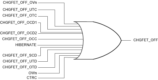
The CHG pin is driven high only when no related faults (OV, OW, OTC, UTC, OTD, UTD, OCD1, OCD2, SCD, OCC, and CTRC disabled) are present and the pack is not in HIBERNATE mode of operation. The CHG pin is used to drive the CHG FET, which is designed to be used on the single device configuration or used by the bottom device in a stack configuration.
Turning off the CHG pin has no influence on the overcurrent protection circuitry. The CHG pin is designed to turn on very quickly; the internal on resistance is about 2 kΩ. The CHG FET turn off relies on the external resistor connected in parallel to the gate-source nodes of the NCH power FET.
The CHG FET may be turned on to protect the FET's body diode if the pack is charging, even if a charging inhibit fault condition is present. This is done through the state comparator. The state comparator (with VSTATE_D threshold and VSTATE_D_HYS hysteresis) remains on for the entire duration of a DSG fault with no CHG fault event.
- If (SRP–SRN) > (VSTATE_D + VSTATE_D_HYS) and no discharge event is detected, the CHG FET output will remain OFF due to the presence of a CHG fault.
- If (SRP–SRN) ≤ VSTATE_D and a discharge event is detected, the CHG FET output will turn ON for body diode protection.
The CHGFET_OFF signal is a result of the presence of any related faults as shown in Figure 9-9.
 Figure 9-9 Faults that Can Qualify CHGFET OFF