SLUSCU0L march 2018 – august 2023 BQ77915
PRODUCTION DATA
- 1
- 1 Features
- 2 Applications
- 3 Description
- 4 Revision History
- 5 Description (continued)
- 6 Device Comparison Table
- 7 Pin Configuration and Functions
- 8 Specifications
-
9 Detailed Description
- 9.1 Overview
- 9.2 Functional Block Diagram
- 9.3
Feature Description
- 9.3.1 Protection Summary
- 9.3.2
Fault Operation
- 9.3.2.1 Operation in OV
- 9.3.2.2 Operation in UV
- 9.3.2.3 Operation in OW
- 9.3.2.4 Operation in OCD1
- 9.3.2.5 Operation in OCD2
- 9.3.2.6 Programming the OCD1/2 Delay Using the OCDP Pin
- 9.3.2.7 Operation in SCD
- 9.3.2.8 Operation in OCC
- 9.3.2.9 Overcurrent Recovery Timer
- 9.3.2.10 Load Detection and Load Removal Detection
- 9.3.2.11 Operation in OTC
- 9.3.2.12 Operation in OTD
- 9.3.2.13 Operation in UTC
- 9.3.2.14 Operation in UTD
- 9.3.3 Protection Response and Recovery Summary
- 9.3.4 Cell Balancing
- 9.3.5 HIBERNATE Mode Operation
- 9.3.6 Configuration CRC Check and Comparator Built-In-Self-Test
- 9.3.7 Fault Detection Method
- 9.3.8 State Comparator
- 9.3.9 DSG FET Driver Operation
- 9.3.10 CHG FET Driver Operation
- 9.3.11 External Override of CHG and DSG Drivers
- 9.3.12 Configuring 3-Series, 4-Series, or 5-Series Modes
- 9.3.13 Stacking Implementations
- 9.3.14 Zero-Volt Battery Charging Inhibition
- 9.4 Device Functional Modes
-
10Application and Implementation
- 10.1
Application Information
- 10.1.1 Recommended System Implementation
- 10.2 Typical Application
- 10.1
Application Information
- 11Power Supply Recommendations
- 12Layout
- 13Device and Documentation Support
- 14Mechanical, Packaging, and Orderable Information
Package Options
Mechanical Data (Package|Pins)
- PW|24
Thermal pad, mechanical data (Package|Pins)
Orderable Information
9.3.9 DSG FET Driver Operation
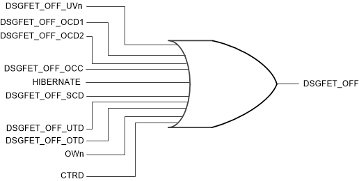
The DSG pin is driven high only when no related faults (UV, OW, OTD, UTD, OCD1, OCD2, SCD, OCC, and CTRD disabled) are present and the device is not in HIBERNATE mode of operation. It is a fast switching driver with a target on resistance of about 15 Ω–20 Ω and an off resistance of RDSGOFF. It is designed to enable customers to select the optimized RGS value to archive the desirable FET rise and fall time per the application requirement and the choice of FET characteristics. When the DSG FET is turned off, the DSG pin drives low and all discharge overcurrent protections (OCD1, OCD2, SCD) are disabled to better conserve power. These resume operation when the DSG FET is turned on. The device provides FET body diode protection through the state comparator if one FET driver is on and the other FET driver is off.
The DSG driver may be turned on to prevent FET damage if the battery pack is charging while a discharge inhibit fault condition is present. This is done by the state comparator. The state comparator (with VSTATE_C threshold and VSTATE_C_HYS hysteresis) remains on for the entire duration of a DSG fault with no CHG fault event.
- If (SRP–SRN) ≤ (VSTATE_C – VSTATE_C_HYS) and no charge event is detected, the DSG FET output will remain OFF due to the presence of a DSG fault.
- If (SRP–SRN) > VSTATE_C and a charge event is detected, the DSG FET output will turn ON for body diode protection.
See State Comparator for details.
The presence of any related faults, as shown in Figure 9-8, results in the DSGFET_OFF signal.
 Figure 9-8 Faults that Can Qualify DSGFET_OFF