SLUSE81E August   2020  – November 2023 BQ79612-Q1 , BQ79614-Q1 , BQ79616-Q1 , BQ79616H-Q1

PRODUCTION DATA  

  1.   1
  2. Features
  3. Applications
  4. Description
  5. Revision History
  6. Description (continued)
  7. Device Comparison Table
  8. Pin Configuration and Functions
  9. Specifications
    1. 8.1 Absolute Maximum Ratings
    2. 8.2 ESD Ratings
    3. 8.3 Recommended Operating Conditions
    4. 8.4 Thermal Information
    5. 8.5 Electrical Characteristics
    6. 8.6 Timing Requirements
    7. 8.7 Typical Characteristics
  10. Detailed Description
    1. 9.1 Overview
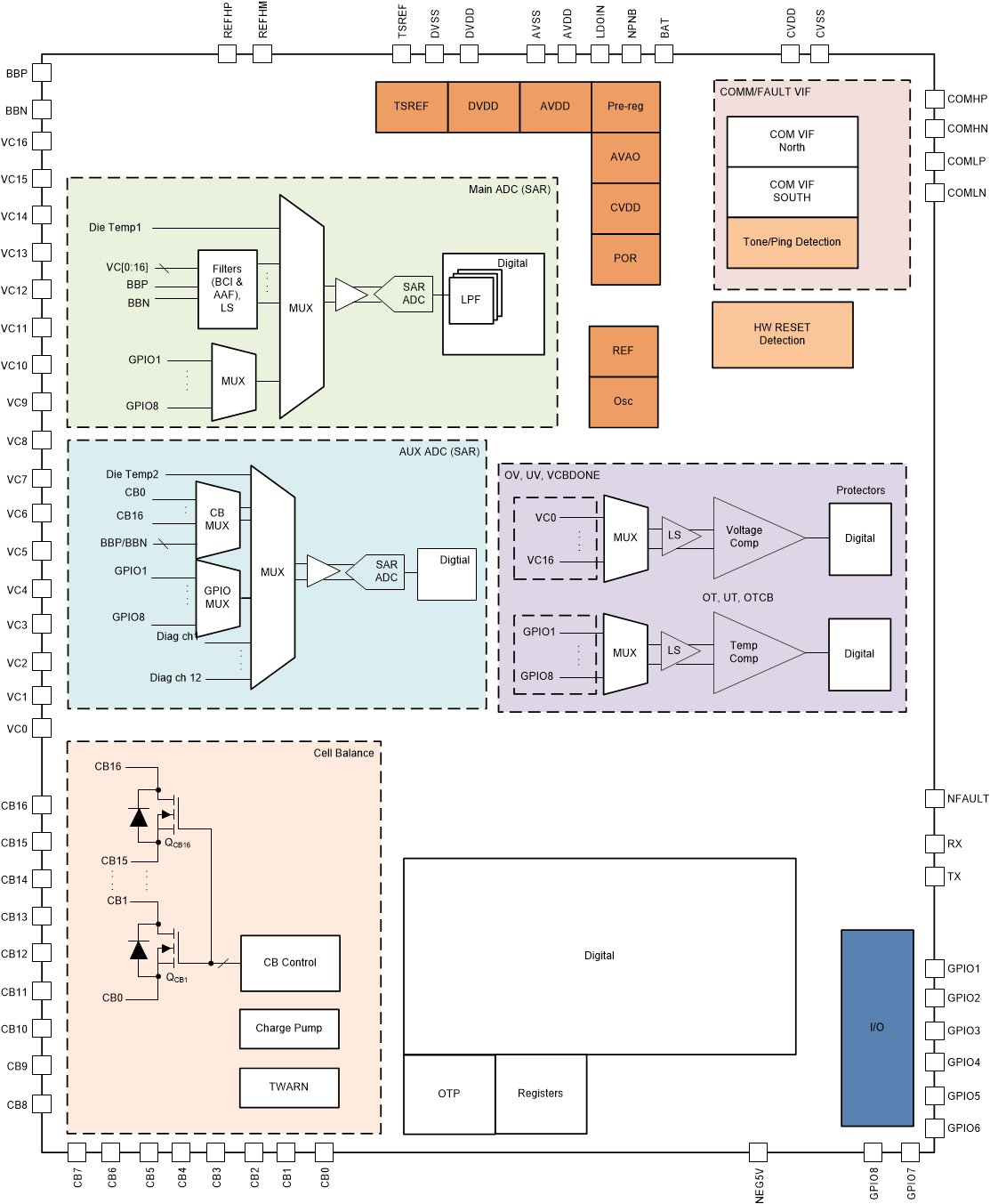
    2. 9.2 Functional Block Diagram
    3. 9.3 Feature Description
      1. 9.3.1 Power Supplies
        1. 9.3.1.1 AVAO_REF and AVDD_REF
        2. 9.3.1.2 LDOIN
        3. 9.3.1.3 AVDD
        4. 9.3.1.4 DVDD
        5. 9.3.1.5 CVDD and NEG5V
        6. 9.3.1.6 TSREF
      2. 9.3.2 Measurement System
        1. 9.3.2.1 Main ADC
          1. 9.3.2.1.1 Cell Voltage Measurements
            1. 9.3.2.1.1.1 Analog Front End
            2. 9.3.2.1.1.2 VC Channel Measurements
            3. 9.3.2.1.1.3 Post-ADC Digital LPF
            4. 9.3.2.1.1.4 BBP and BBN Measurements
          2. 9.3.2.1.2 Temperature Measurements
            1. 9.3.2.1.2.1 DieTemp1 Measurement
            2. 9.3.2.1.2.2 GPIOs and TSREF Measurements
          3. 9.3.2.1.3 Main ADC Operation Control
            1. 9.3.2.1.3.1 Operation Modes and Status
        2. 9.3.2.2 AUX ADC
          1. 9.3.2.2.1 AUX Cell Voltage Measurements
            1. 9.3.2.2.1.1 AUX Analog Front End
            2. 9.3.2.2.1.2 CB and BB Channel Measurements
          2. 9.3.2.2.2 AUX Temperature Measurements
            1. 9.3.2.2.2.1 DieTemp2 Measurement
            2. 9.3.2.2.2.2 AUX GPIO Measurements
          3. 9.3.2.2.3 MISC Measurements
          4. 9.3.2.2.4 AUX ADC Operation Control
        3. 9.3.2.3 Synchronization between MAIN and AUX ADC Measurements
      3. 9.3.3 Cell Balancing
        1. 9.3.3.1 Set Up Cell Balancing
          1. 9.3.3.1.1 Step 1: Determine Balancing Channels
          2. 9.3.3.1.2 Step 2: Select Balancing Control Methods
          3. 9.3.3.1.3 Step 3a: Balancing Thermal Management
          4. 9.3.3.1.4 Step 3b: Option to Stop On Cell Voltage Threshold
          5. 9.3.3.1.5 Step 3c: Option to Stop at Fault
        2. 9.3.3.2 Cell Balancing in SLEEP Mode
        3. 9.3.3.3 Pause and Stop Cell Balancing
          1. 9.3.3.3.1 Cell Balancing Pause
          2. 9.3.3.3.2 Cell Balancing Stop
          3. 9.3.3.3.3 Remaining CB Time
        4. 9.3.3.4 Module Balancing
          1. 9.3.3.4.1 Start Module Balancing
          2. 9.3.3.4.2 Stop Module Balancing
      4. 9.3.4 Integrated Hardware Protectors
        1. 9.3.4.1 OVUV Protectors
          1. 9.3.4.1.1 OVUV Operation Modes
          2. 9.3.4.1.2 OVUV Control and Status
            1. 9.3.4.1.2.1 OVUV Control
            2. 9.3.4.1.2.2 OVUV Status
        2. 9.3.4.2 OTUT Protector
          1. 9.3.4.2.1 OTUT Operation Modes
          2. 9.3.4.2.2 OTUT Control and Status
            1. 9.3.4.2.2.1 OTUT Control
            2. 9.3.4.2.2.2 OTUT Status
      5. 9.3.5 GPIO Configuration
      6. 9.3.6 Communication, OTP, Diagnostic Control
        1. 9.3.6.1 Communication
          1. 9.3.6.1.1 Serial Interface
            1. 9.3.6.1.1.1 UART Physical Layer
              1. 9.3.6.1.1.1.1 UART Transmitter
              2. 9.3.6.1.1.1.2 UART Receiver
              3. 9.3.6.1.1.1.3 COMM CLEAR
            2. 9.3.6.1.1.2 Command and Response Protocol
              1. 9.3.6.1.1.2.1 Transaction Frame Structure
                1. 9.3.6.1.1.2.1.1 Frame Initialization Byte
                2. 9.3.6.1.1.2.1.2 Device Address Byte
                3. 9.3.6.1.1.2.1.3 Register Address Bytes
                4. 9.3.6.1.1.2.1.4 Data Bytes
                5. 9.3.6.1.1.2.1.5 CRC Bytes
                6. 9.3.6.1.1.2.1.6 Calculating Frame CRC Value
                7. 9.3.6.1.1.2.1.7 Verifying Frame CRC
              2. 9.3.6.1.1.2.2 Transaction Frame Examples
                1. 9.3.6.1.1.2.2.1 Single Device Read/Write
                2. 9.3.6.1.1.2.2.2 Stack Read/Write
                3. 9.3.6.1.1.2.2.3 Broadcast Read/Write
                4. 9.3.6.1.1.2.2.4 Broadcast Write Reverse Direction
          2. 9.3.6.1.2 Daisy Chain Interface
            1. 9.3.6.1.2.1 Daisy Chain Transmitter and Receiver Functionality
            2. 9.3.6.1.2.2 Daisy Chain Protocol
          3. 9.3.6.1.3 Start Communication
            1. 9.3.6.1.3.1 Identify Base and Stack
            2. 9.3.6.1.3.2 Auto-Addressing
              1. 9.3.6.1.3.2.1 Setting Up the Device Addresses
              2. 9.3.6.1.3.2.2 Setting Up COMM_CTRL[STACK_DEV] and [TOP_STACK]
              3. 9.3.6.1.3.2.3 Storing Device Address to OTP
            3. 9.3.6.1.3.3 Synchronize Daisy Chain DLL
            4. 9.3.6.1.3.4 Ring Communication
          4. 9.3.6.1.4 Communication Timeout
            1. 9.3.6.1.4.1 Short Communication Timeout
            2. 9.3.6.1.4.2 Long Communication Timeout
          5. 9.3.6.1.5 Communication Debug Mode
          6. 9.3.6.1.6 Multidrop Configuration
          7. 9.3.6.1.7 SPI Master
          8. 9.3.6.1.8 SPI Loopback
        2. 9.3.6.2 Fault Handling
          1. 9.3.6.2.1 Fault Status Hierarchy
            1. 9.3.6.2.1.1 Debug Registers
          2. 9.3.6.2.2 Fault Masking and Reset
            1. 9.3.6.2.2.1 Fault Masking
            2. 9.3.6.2.2.2 Fault Reset
          3. 9.3.6.2.3 Fault Signaling
            1. 9.3.6.2.3.1 Fault Status Transmitting in ACTIVE Mode
            2. 9.3.6.2.3.2 Fault Status Transmitting in SLEEP Mode
            3. 9.3.6.2.3.3 Heartbeat and Fault Tone
        3. 9.3.6.3 Nonvolatile Memory
          1. 9.3.6.3.1 OTP Page Status
          2. 9.3.6.3.2 OTP Programming
        4. 9.3.6.4 Diagnostic Control/Status
          1. 9.3.6.4.1 Power Supplies Check
            1. 9.3.6.4.1.1 Power Supply Diagnostic Check
            2. 9.3.6.4.1.2 Power Supply BIST
          2. 9.3.6.4.2 Thermal Shutdown and Warning Check
            1. 9.3.6.4.2.1 Thermal Shutdown
            2. 9.3.6.4.2.2 Thermal Warning
          3. 9.3.6.4.3 Oscillators Watchdog
          4. 9.3.6.4.4 OTP Error Check
            1. 9.3.6.4.4.1 OTP CRC Test and Faults
            2. 9.3.6.4.4.2 OTP Margin Read
            3. 9.3.6.4.4.3 Error Check and Correct (ECC) OTP
          5. 9.3.6.4.5 Integrated Hardware Protector Check
            1. 9.3.6.4.5.1 Parity Check
            2. 9.3.6.4.5.2 OVUV and OTUT DAC Check
            3. 9.3.6.4.5.3 OVUV Protector BIST
            4. 9.3.6.4.5.4 OTUT Protector BIST
          6. 9.3.6.4.6 Diagnostic Through ADC Comparison
            1. 9.3.6.4.6.1 Cell Voltage Measurement Check
            2. 9.3.6.4.6.2 Temperature Measurement Check
            3. 9.3.6.4.6.3 Cell Balancing FETs Check
            4. 9.3.6.4.6.4 VC and CB Open Wire Check
      7. 9.3.7 Bus Bar Support
        1. 9.3.7.1 Bus Bar on BBP/BBN Pins
          1. 9.3.7.1.1 Typical Connection
          2. 9.3.7.1.2 Bus Bar Measurement
          3. 9.3.7.1.3 Cell Balancing Handling
          4. 9.3.7.1.4 Cell Voltage Diagnostic Control
        2. 9.3.7.2 Bus Bar on Individual VC Channel
          1. 9.3.7.2.1 Typical Connection
          2. 9.3.7.2.2 Bus Bar Measurement
          3. 9.3.7.2.3 Cell Balancing Handling
          4. 9.3.7.2.4 Cell Voltage Diagnostic Control
    4. 9.4 Device Functional Modes
      1. 9.4.1 Power Modes
        1. 9.4.1.1 SHUTDOWN Mode
          1. 9.4.1.1.1 Exit SHUTDOWN Mode
          2. 9.4.1.1.2 Enter SHUTDOWN Mode
        2. 9.4.1.2 SLEEP Mode
          1. 9.4.1.2.1 Exit SLEEP Mode
          2. 9.4.1.2.2 Enter SLEEP Mode
        3. 9.4.1.3 ACTIVE Mode
          1. 9.4.1.3.1 Exit ACTIVE Mode
          2. 9.4.1.3.2 Enter ACTIVE Mode From SHUTDOWN Mode
          3. 9.4.1.3.3 Enter ACTIVE Mode From SLEEP Mode
      2. 9.4.2 Device Reset
      3. 9.4.3 Ping and Tone
        1. 9.4.3.1 Ping
        2. 9.4.3.2 Tone
        3. 9.4.3.3 Ping and Tone Propagation
    5. 9.5 Register Maps
      1. 9.5.1 OTP Shadow Register Summary
      2. 9.5.2 Read/Write Register Summary
      3. 9.5.3 Read-Only Register Summary
      4. 9.5.4 Register Field Descriptions
        1. 9.5.4.1  Device Addressing Setup
          1. 9.5.4.1.1 DIR0_ADDR_OTP
          2. 9.5.4.1.2 DIR1_ADDR_OTP
          3. 9.5.4.1.3 CUST_MISC1 through CUST_MISC8
          4. 9.5.4.1.4 DIR0_ADDR
          5. 9.5.4.1.5 DIR1_ADDR
        2. 9.5.4.2  Device ID and Scratch Pad
          1. 9.5.4.2.1 PARTID
          2. 9.5.4.2.2 DEV_REVID
          3. 9.5.4.2.3 DIE_ID1 through DIE_ID9
        3. 9.5.4.3  General Configuration and Control
          1. 9.5.4.3.1  DEV_CONF
          2. 9.5.4.3.2  ACTIVE_CELL
          3. 9.5.4.3.3  BBVC_POSN1
          4. 9.5.4.3.4  BBVC_POSN2
          5. 9.5.4.3.5  PWR_TRANSIT_CONF
          6. 9.5.4.3.6  COMM_TIMEOUT_CONF
          7. 9.5.4.3.7  TX_HOLD_OFF
          8. 9.5.4.3.8  STACK_RESPONSE
          9. 9.5.4.3.9  BBP_LOC
          10. 9.5.4.3.10 COMM_CTRL
          11. 9.5.4.3.11 CONTROL1
          12. 9.5.4.3.12 CONTROL2
          13. 9.5.4.3.13 CUST_CRC_HI
          14. 9.5.4.3.14 CUST_CRC_LO
          15. 9.5.4.3.15 CUST_CRC_RSLT_HI
          16. 9.5.4.3.16 CUST_CRC_RSLT_LO
        4. 9.5.4.4  Operation Status
          1. 9.5.4.4.1 DIAG_STAT
          2. 9.5.4.4.2 ADC_STAT1
          3. 9.5.4.4.3 ADC_STAT2
          4. 9.5.4.4.4 GPIO_STAT
          5. 9.5.4.4.5 BAL_STAT
          6. 9.5.4.4.6 DEV_STAT
        5. 9.5.4.5  ADC Configuration and Control
          1. 9.5.4.5.1 ADC_CONF1
          2. 9.5.4.5.2 ADC_CONF2
          3. 9.5.4.5.3 MAIN_ADC_CAL1
          4. 9.5.4.5.4 MAIN_ADC_CAL2
          5. 9.5.4.5.5 AUX_ADC_CAL1
          6. 9.5.4.5.6 AUX_ADC_CAL2
          7. 9.5.4.5.7 ADC_CTRL1
          8. 9.5.4.5.8 ADC_CTRL2
          9. 9.5.4.5.9 ADC_CTRL3
        6. 9.5.4.6  ADC Measurement Results
          1. 9.5.4.6.1  VCELL16_HI/LO
          2. 9.5.4.6.2  VCELL15_HI/LO
          3. 9.5.4.6.3  VCELL14_HI/LO
          4. 9.5.4.6.4  VCELL13_HI/LO
          5. 9.5.4.6.5  VCELL12_HI/LO
          6. 9.5.4.6.6  VCELL11_HI/LO
          7. 9.5.4.6.7  VCELL10_HI/LO
          8. 9.5.4.6.8  VCELL9_HI/LO
          9. 9.5.4.6.9  VCELL8_HI/LO
          10. 9.5.4.6.10 VCELL7_HI/LO
          11. 9.5.4.6.11 VCELL6_HI/LO
          12. 9.5.4.6.12 VCELL5_HI/LO
          13. 9.5.4.6.13 VCELL4_HI/LO
          14. 9.5.4.6.14 VCELL3_HI/LO
          15. 9.5.4.6.15 VCELL2_HI/LO
          16. 9.5.4.6.16 VCELL1_HI/LO
          17. 9.5.4.6.17 BUSBAR_HI/LO
          18. 9.5.4.6.18 TSREF_HI/LO
          19. 9.5.4.6.19 GPIO1_HI/LO
          20. 9.5.4.6.20 GPIO2_HI/LO
          21. 9.5.4.6.21 GPIO3_HI/LO
          22. 9.5.4.6.22 GPIO4_HI/LO
          23. 9.5.4.6.23 GPIO5_HI/LO
          24. 9.5.4.6.24 GPIO6_HI/LO
          25. 9.5.4.6.25 GPIO7_HI/LO
          26. 9.5.4.6.26 GPIO8_HI/LO
          27. 9.5.4.6.27 DIETEMP1_HI/LO
          28. 9.5.4.6.28 DIETEMP2_HI/LO
          29. 9.5.4.6.29 AUX_CELL_HI/LO
          30. 9.5.4.6.30 AUX_GPIO_HI/LO
          31. 9.5.4.6.31 AUX_BAT_HI/LO
          32. 9.5.4.6.32 AUX_REFL_HI/LO
          33. 9.5.4.6.33 AUX_VBG2_HI/LO
          34. 9.5.4.6.34 AUX_AVAO_REF_HI/LO
          35. 9.5.4.6.35 AUX_AVDD_REF_HI/LO
          36. 9.5.4.6.36 AUX_OV_DAC_HI/LO
          37. 9.5.4.6.37 AUX_UV_DAC_HI/LO
          38. 9.5.4.6.38 AUX_OT_OTCB_DAC_HI/LO
          39. 9.5.4.6.39 AUX_UT_DAC_HI/LO
          40. 9.5.4.6.40 AUX_VCBDONE_DAC_HI/LO
          41. 9.5.4.6.41 AUX_VCM_HI/LO
          42. 9.5.4.6.42 REFOVDAC_HI/LO
          43. 9.5.4.6.43 DIAG_MAIN_HI/LO
          44. 9.5.4.6.44 DIAG_AUX_HI/LO
        7. 9.5.4.7  Balancing Configuration, Control and Status
          1. 9.5.4.7.1  CB_CELL16_CTRL through CB_CELL1_CTRL
          2. 9.5.4.7.2  VMB_DONE_THRESH
          3. 9.5.4.7.3  MB_TIMER_CTRL
          4. 9.5.4.7.4  VCB_DONE_THRESH
          5. 9.5.4.7.5  OTCB_THRESH
          6. 9.5.4.7.6  BAL_CTRL1
          7. 9.5.4.7.7  BAL_CTRL2
          8. 9.5.4.7.8  BAL_CTRL3
          9. 9.5.4.7.9  CB_COMPLETE1
          10. 9.5.4.7.10 CB_COMPLETE2
          11. 9.5.4.7.11 BAL_TIME
        8. 9.5.4.8  Protector Configuration and Control
          1. 9.5.4.8.1 OV_THRESH
          2. 9.5.4.8.2 UV_THRESH
          3. 9.5.4.8.3 UV_DISABLE1
          4. 9.5.4.8.4 UV_DISABLE2
          5. 9.5.4.8.5 OTUT_THRESH
          6. 9.5.4.8.6 OVUV_CTRL
          7. 9.5.4.8.7 OTUT_CTRL
        9. 9.5.4.9  GPIO Configuration
          1. 9.5.4.9.1 GPIO_CONF1
          2. 9.5.4.9.2 GPIO_CONF2
          3. 9.5.4.9.3 GPIO_CONF3
          4. 9.5.4.9.4 GPIO_CONF4
        10. 9.5.4.10 SPI Master
          1. 9.5.4.10.1 SPI_CONF
          2. 9.5.4.10.2 SPI_EXE
          3. 9.5.4.10.3 SPI_TX3, SPI_TX2, and SPI_TX1
          4. 9.5.4.10.4 SPI_RX3, SPI_RX2, and SPI_RX1
        11. 9.5.4.11 Diagnostic Control
          1. 9.5.4.11.1  DIAG_OTP_CTRL
          2. 9.5.4.11.2  DIAG_COMM_CTRL
          3. 9.5.4.11.3  DIAG_PWR_CTRL
          4. 9.5.4.11.4  DIAG_CBFET_CTRL1
          5. 9.5.4.11.5  DIAG_CBFET_CTRL2
          6. 9.5.4.11.6  DIAG_COMP_CTRL1
          7. 9.5.4.11.7  DIAG_COMP_CTRL2
          8. 9.5.4.11.8  DIAG_COMP_CTRL3
          9. 9.5.4.11.9  DIAG_COMP_CTRL4
          10. 9.5.4.11.10 DIAG_PROT_CTRL
        12. 9.5.4.12 Fault Configuration and Reset
          1. 9.5.4.12.1 FAULT_MSK1
          2. 9.5.4.12.2 FAULT_MSK2
          3. 9.5.4.12.3 FAULT_RST1
          4. 9.5.4.12.4 FAULT_RST2
        13. 9.5.4.13 Fault Status
          1. 9.5.4.13.1  FAULT_SUMMARY
          2. 9.5.4.13.2  FAULT_COMM1
          3. 9.5.4.13.3  FAULT_COMM2
          4. 9.5.4.13.4  FAULT_COMM3
          5. 9.5.4.13.5  FAULT_OTP
          6. 9.5.4.13.6  FAULT_SYS
          7. 9.5.4.13.7  FAULT_PROT1
          8. 9.5.4.13.8  FAULT_PROT2
          9. 9.5.4.13.9  FAULT_OV1
          10. 9.5.4.13.10 FAULT_OV2
          11. 9.5.4.13.11 FAULT_UV1
          12. 9.5.4.13.12 FAULT_UV2
          13. 9.5.4.13.13 FAULT_OT
          14. 9.5.4.13.14 FAULT_UT
          15. 9.5.4.13.15 FAULT_COMP_GPIO
          16. 9.5.4.13.16 FAULT_COMP_VCCB1
          17. 9.5.4.13.17 FAULT_COMP_VCCB2
          18. 9.5.4.13.18 FAULT_COMP_VCOW1
          19. 9.5.4.13.19 FAULT_COMP_VCOW2
          20. 9.5.4.13.20 FAULT_COMP_CBOW1
          21. 9.5.4.13.21 FAULT_COMP_CBOW2
          22. 9.5.4.13.22 FAULT_COMP_CBFET1
          23. 9.5.4.13.23 FAULT_COMP_CBFET2
          24. 9.5.4.13.24 FAULT_COMP_MISC
          25. 9.5.4.13.25 FAULT_PWR1
          26. 9.5.4.13.26 FAULT_PWR2
          27. 9.5.4.13.27 FAULT_PWR3
        14. 9.5.4.14 Debug Control and Status
          1. 9.5.4.14.1  DEBUG_CTRL_UNLOCK
          2. 9.5.4.14.2  DEBUG_COMM_CTRL1
          3. 9.5.4.14.3  DEBUG_COMM_CTRL2
          4. 9.5.4.14.4  DEBUG_COMM_STAT
          5. 9.5.4.14.5  DEBUG_UART_RC
          6. 9.5.4.14.6  DEBUG_UART_RR_TR
          7. 9.5.4.14.7  DEBUG_COMH_BIT
          8. 9.5.4.14.8  DEBUG_COMH_RC
          9. 9.5.4.14.9  DEBUG_COMH_RR_TR
          10. 9.5.4.14.10 DEBUG_COML_BIT
          11. 9.5.4.14.11 DEBUG_COML_RC
          12. 9.5.4.14.12 DEBUG_COML_RR_TR
          13. 9.5.4.14.13 DEBUG_UART_DISCARD
          14. 9.5.4.14.14 DEBUG_COMH_DISCARD
          15. 9.5.4.14.15 DEBUG_COML_DISCARD
          16. 9.5.4.14.16 DEBUG_UART_VALID_HI/LO
          17. 9.5.4.14.17 DEBUG_COMH_VALID_HI/LO
          18. 9.5.4.14.18 DEBUG_COML_VALID_HI/LO
          19. 9.5.4.14.19 DEBUG_OTP_SEC_BLK
          20. 9.5.4.14.20 DEBUG_OTP_DED_BLK
        15. 9.5.4.15 OTP Programming Control and Status
          1. 9.5.4.15.1 OTP_PROG_UNLOCK1A through OTP_PROG_UNLOCK1D
          2. 9.5.4.15.2 OTP_PROG_UNLOCK2A through OTP_PROG_UNLOCK2D
          3. 9.5.4.15.3 OTP_PROG_CTRL
          4. 9.5.4.15.4 OTP_ECC_TEST
          5. 9.5.4.15.5 OTP_ECC_DATAIN1 through OTP_ECC_DATAIN9
          6. 9.5.4.15.6 OTP_ECC_DATAOUT1 through OTP_ECC_DATAOUT9
          7. 9.5.4.15.7 OTP_PROG_STAT
          8. 9.5.4.15.8 OTP_CUST1_STAT
          9. 9.5.4.15.9 OTP_CUST2_STAT
  11. 10Application and Implementation
    1. 10.1 Application Information
    2. 10.2 Typical Applications
      1. 10.2.1 Base Device Application Circuit
        1. 10.2.1.1 Design Requirements
        2. 10.2.1.2 Detailed Design Procedure
          1. 10.2.1.2.1 Cell Sensing and Balancing Inputs
          2. 10.2.1.2.2 BAT and External NPN
          3. 10.2.1.2.3 Power Supplies, Reference Input
          4. 10.2.1.2.4 GPIO For Thermistor Inputs
          5. 10.2.1.2.5 Internal Balancing Current
          6. 10.2.1.2.6 UART, NFAULT
          7. 10.2.1.2.7 Daisy Chain Isolation
            1. 10.2.1.2.7.1 Devices Connected on the Same PCB
            2. 10.2.1.2.7.2 Devices Connected on Different PCBs
        3. 10.2.1.3 Application Curve
      2. 10.2.2 Daisy Device Application Circuit
        1. 10.2.2.1 Design Requirements
        2. 10.2.2.2 Detailed Design Procedure
  12. 11Power Supply Recommendations
  13. 12Layout
    1. 12.1 Layout Guidelines
      1. 12.1.1 Ground Planes
      2. 12.1.2 Bypass Capacitors for Power Supplies and Reference
      3. 12.1.3 Cell Voltage Sensing
      4. 12.1.4 Daisy Chain Communication
    2. 12.2 Layout Example
  14. 13Device and Documentation Support
    1. 13.1 Device Support
      1. 13.1.1 Third-Party Products Disclaimer
    2. 13.2 Receiving Notification of Documentation Updates
    3. 13.3 Support Resources
    4. 13.4 Trademarks
    5. 13.5 Electrostatic Discharge Caution
    6. 13.6 Glossary
  15. 14Mechanical, Packaging, and Orderable Information

Package Options

Mechanical Data (Package|Pins)
Thermal pad, mechanical data (Package|Pins)
Orderable Information

Functional Block Diagram

The BQ79616 functional block diagram also applies to BQ79616H, BQ79614 and BQ79612 but with fewer VC and CB input channels.

GUID-FF5FB16E-DA08-4D77-A3B9-E9DBB55C2735-low.gif