SBOS571C August   2011  – August 2018 BUF20800-Q1

PRODUCTION DATA.  

  1. Features
  2. Applications
  3. Description
    1.     Device Images
      1.      Simplified Block Diagram
  4. Revision History
  5. Pin Configuration and Functions
    1.     Pin Functions
  6. Specifications
    1. 6.1 Absolute Maximum Ratings
    2. 6.2 ESD Ratings
    3. 6.3 Recommended Operating Conditions
    4. 6.4 Thermal Information
    5. 6.5 Electrical Characteristics
    6. 6.6 Typical Characteristics
  7. Detailed Description
    1. 7.1 Overview
    2. 7.2 Functional Block Diagram
    3. 7.3 Feature Description
      1. 7.3.1 General-call Reset and Power-up
      2. 7.3.2 Output Voltage
      3. 7.3.3 Output Latch
      4. 7.3.4 Programmable VCOM
      5. 7.3.5 REFH and REFL Input range
    4. 7.4 Device Functional Modes
      1. 7.4.1 Replacement of Traditional Gamma Buffer
      2. 7.4.2 Dynamic Gamma Control
    5. 7.5 Programming
      1. 7.5.1 Two-wire Bus Overview
      2. 7.5.2 Data Rates
      3. 7.5.3 Read/Write Operations
        1. 7.5.3.1 Writing
        2. 7.5.3.2 Reading
      4. 7.5.4 Register Maps
        1. 7.5.4.1 Addressing the BUF20800-Q1
      5. 7.5.5 Registers
  8. Application and Implementation
    1. 8.1 Application Information
    2. 8.2 Typical Application
      1. 8.2.1 Design Requirements
      2. 8.2.2 Detailed Design Procedure
        1. 8.2.2.1 Input Capacitor Selection
        2. 8.2.2.2 REFH and REFL Voltage Settings
      3. 8.2.3 Application Curves
      4. 8.2.4 Configuration for 20 Gamma Channels
      5. 8.2.5 Configuration for 22 Gamma Channels
      6. 8.2.6 The BUF20800-Q1 in Industrial Applications
      7. 8.2.7 Total TI Panel Solution
  9. Power Supply Recommendations
  10. 10Layout
    1. 10.1 Layout Guidelines
      1. 10.1.1 General PowerPAD Design Considerations
    2. 10.2 Layout Example
  11. 11Device and Documentation Support
    1. 11.1 Documentation Support
      1. 11.1.1 Related Documentation
    2. 11.2 Receiving Notification of Documentation Updates
    3. 11.3 Community Resources
    4. 11.4 Trademarks
    5. 11.5 Electrostatic Discharge Caution
    6. 11.6 Glossary
  12. 12Mechanical, Packaging, and Orderable Information

Package Options

Mechanical Data (Package|Pins)
Thermal pad, mechanical data (Package|Pins)
Orderable Information

Configuration for 20 Gamma Channels

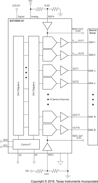
The VCOM outputs can be used as additional gamma references in order to achieve two additional gamma channels (20 total). The VCOM outputs will behave the same as the OUT1−9 outputs when sourcing or sinking smaller currents (see Figure 4). The VCOM outputs are better able to swing to the positive rail than to the negative rail. Therefore, it is better to use the VCOM outputs for higher reference voltages, as shown in Figure 17.
BUF20800-Q1 appinfo_20gammasoln_SBOS571.gifFigure 17. 20 Gamma Channel Solution − Two VCOM Channels Used as Additional Gamma Channels