SBOS571C August   2011  – August 2018 BUF20800-Q1

PRODUCTION DATA.  

  1. Features
  2. Applications
  3. Description
    1.     Device Images
      1.      Simplified Block Diagram
  4. Revision History
  5. Pin Configuration and Functions
    1.     Pin Functions
  6. Specifications
    1. 6.1 Absolute Maximum Ratings
    2. 6.2 ESD Ratings
    3. 6.3 Recommended Operating Conditions
    4. 6.4 Thermal Information
    5. 6.5 Electrical Characteristics
    6. 6.6 Typical Characteristics
  7. Detailed Description
    1. 7.1 Overview
    2. 7.2 Functional Block Diagram
    3. 7.3 Feature Description
      1. 7.3.1 General-call Reset and Power-up
      2. 7.3.2 Output Voltage
      3. 7.3.3 Output Latch
      4. 7.3.4 Programmable VCOM
      5. 7.3.5 REFH and REFL Input range
    4. 7.4 Device Functional Modes
      1. 7.4.1 Replacement of Traditional Gamma Buffer
      2. 7.4.2 Dynamic Gamma Control
    5. 7.5 Programming
      1. 7.5.1 Two-wire Bus Overview
      2. 7.5.2 Data Rates
      3. 7.5.3 Read/Write Operations
        1. 7.5.3.1 Writing
        2. 7.5.3.2 Reading
      4. 7.5.4 Register Maps
        1. 7.5.4.1 Addressing the BUF20800-Q1
      5. 7.5.5 Registers
  8. Application and Implementation
    1. 8.1 Application Information
    2. 8.2 Typical Application
      1. 8.2.1 Design Requirements
      2. 8.2.2 Detailed Design Procedure
        1. 8.2.2.1 Input Capacitor Selection
        2. 8.2.2.2 REFH and REFL Voltage Settings
      3. 8.2.3 Application Curves
      4. 8.2.4 Configuration for 20 Gamma Channels
      5. 8.2.5 Configuration for 22 Gamma Channels
      6. 8.2.6 The BUF20800-Q1 in Industrial Applications
      7. 8.2.7 Total TI Panel Solution
  9. Power Supply Recommendations
  10. 10Layout
    1. 10.1 Layout Guidelines
      1. 10.1.1 General PowerPAD Design Considerations
    2. 10.2 Layout Example
  11. 11Device and Documentation Support
    1. 11.1 Documentation Support
      1. 11.1.1 Related Documentation
    2. 11.2 Receiving Notification of Documentation Updates
    3. 11.3 Community Resources
    4. 11.4 Trademarks
    5. 11.5 Electrostatic Discharge Caution
    6. 11.6 Glossary
  12. 12Mechanical, Packaging, and Orderable Information

Package Options

Mechanical Data (Package|Pins)
Thermal pad, mechanical data (Package|Pins)
Orderable Information

Configuration for 22 Gamma Channels

In addition to the VCOM outputs, the REFH and REFL OUT outputs can also be used as fixed gamma references. The output voltage will be set by the REFH and REFL input voltages, respectively. Therefore, REFH OUT should be used for the highest voltage gamma reference, and REFL OUT for the lowest voltage gamma reference. A 22-channel solution can be created by using all 18 outputs, the two VCOM outputs, and both REFH/L OUT outputs for gamma references—see Figure 15. However, the REFH and REFL OUT buffers were designed to only drive light loads on the order of 5−10mA. Driving capacitive loads is not recommended with these buffers. In addition, the REFH and REFL buffers must not be allowed to saturate from sourcing/sinking too much current from REFH OUT or REFL OUT. Saturation of the REFH and REFL buffers results in errors in the voltages of OUT1−18 and VCOM OUT1−2. The BUF01900 can be used to provide a programmable VCOM output.
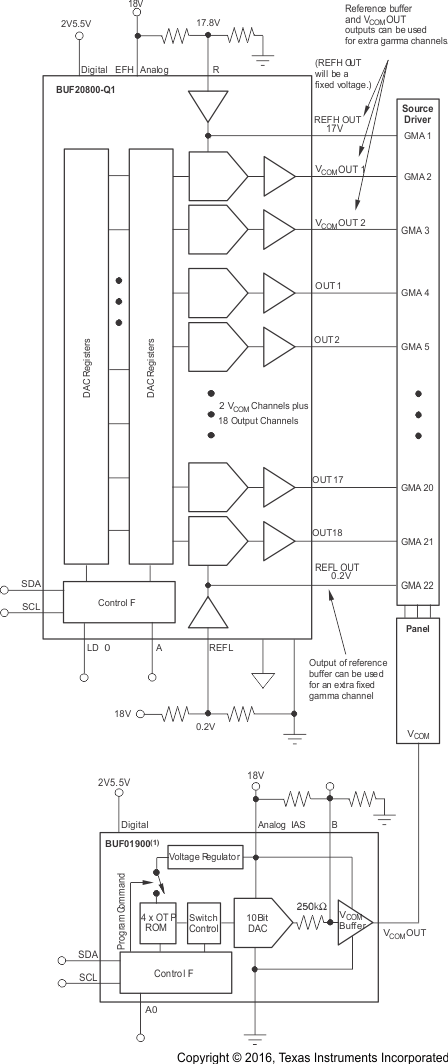
BUF20800-Q1 appinfo_22chsoln_SBOS571.gifFigure 18. 22-Channel Gamma Solution