SBOS571C August 2011 – August 2018 BUF20800-Q1
PRODUCTION DATA.
- 1 Features
- 2 Applications
- 3 Description
- 4 Revision History
- 5 Pin Configuration and Functions
- 6 Specifications
- 7 Detailed Description
- 8 Application and Implementation
- 9 Power Supply Recommendations
- 10Layout
- 11Device and Documentation Support
- 12Mechanical, Packaging, and Orderable Information
Package Options
Mechanical Data (Package|Pins)
- DCP|38
Thermal pad, mechanical data (Package|Pins)
- DCP|38
Orderable Information
8.2.6 The BUF20800-Q1 in Industrial Applications
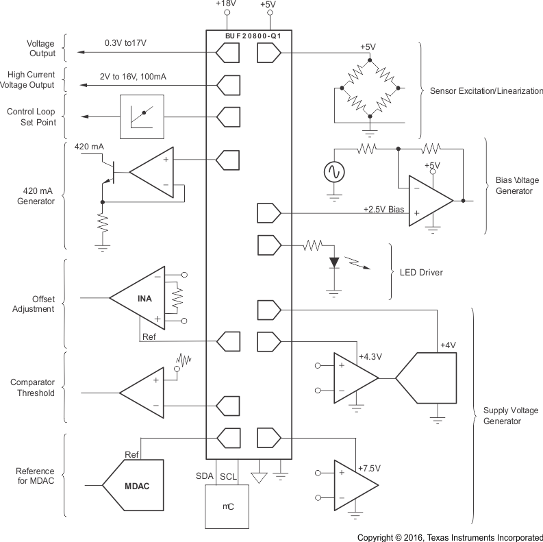
The wide supply range, high output current, and very low cost make the BUF20800-Q1 attractive for a range of medium accuracy industrial applications such as programmable power supplies, multi-channel data-acquisition systems, data loggers, sensor excitation and linearization, power-supply generation, and other uses. Each DAC channel features 1LSB DNL and INL.
Many systems require different levels of biasing and power supply for various components as well as sensor excitation, control-loop set-points, voltage outputs, current outputs, and other functions. The BUF20800-Q1, with its 20 total programmable DAC channels, provides great flexibility to the entire system by allowing the designer to change all these parameters via software.
Figure 19 provides various ideas on how the BUF20800-Q1 can be used in applications. A micro-controller with two-wire serial interface controls the various DACs of the BUF20800-Q1. The BUF20800-Q1 can be used for:
- sensor excitation
- programmable bias/reference voltages
- variable power-supplies
- high-current voltage output
- 4-20mA output
- set-point generators for control loops
NOTE: The output voltages of the BUF20800-Q1 DACs will be set to (VREFH − VREFL)/2 at power-up or reset.
 Figure 19. Industrial Applications for the BUF20800-Q1