SBOS948F February   2019  – May 2021 BUF634A

PRODUCTION DATA  

  1. Features
  2. Applications
  3. Description
  4. Revision History
  5. Device Comparison Table
  6. Pin Configuration and Functions
  7. Specifications
    1. 7.1 Absolute Maximum Ratings
    2. 7.2 ESD Ratings
    3. 7.3 Recommended Operating Conditions
    4. 7.4 Thermal Information
    5. 7.5 Electrical Characteristics: Wide-Bandwidth Mode
    6. 7.6 Electrical Characteristics: Low-Quiescent Current Mode
    7. 7.7 Typical Characteristics
  8. Detailed Description
    1. 8.1 Overview
    2. 8.2 Functional Block Diagram
    3. 8.3 Feature Description
      1. 8.3.1 Output Current
      2. 8.3.2 Thermal Shutdown
      3. 8.3.3 ESD Protection
    4. 8.4 Device Functional Modes
      1. 8.4.1 Adjustable Bandwidth
  9. Application and Implementation
    1. 9.1 Application Information
      1. 9.1.1 High-Frequency Applications
    2. 9.2 Typical Application
      1. 9.2.1 Design Requirements
      2. 9.2.2 Detailed Design Procedure
      3. 9.2.3 Application Curves
  10. 10Power Supply Recommendations
    1. 10.1 Power Dissipation and Thermal Considerations
  11. 11Layout
    1. 11.1 Layout Guidelines
      1. 11.1.1 SOIC Layout Guidelines (D Package Without a Thermal Pad)
      2. 11.1.2 HSOIC Layout Guidelines (DDA Package With a Thermal Pad)
    2. 11.2 Layout Example
  12. 12Device and Documentation Support
    1. 12.1 Device Support
      1. 12.1.1 Third-Party Products Disclaimer
      2. 12.1.2 Development Support
        1. 12.1.2.1 TINA-TI (Free Software Download)
        2. 12.1.2.2 TI Precision Designs
    2. 12.2 Documentation Support
      1. 12.2.1 Related Documentation
    3. 12.3 Receiving Notification of Documentation Updates
    4. 12.4 Support Resources
    5. 12.5 Trademarks
    6. 12.6 Electrostatic Discharge Caution
    7. 12.7 Glossary
  13. 13Mechanical, Packaging, and Orderable Information

Package Options

Refer to the PDF data sheet for device specific package drawings

Mechanical Data (Package|Pins)
  • D|8
  • DDA|8
  • DRB|8
Thermal pad, mechanical data (Package|Pins)
Orderable Information

Functional Block Diagram

GUID-2F8A7DA1-6829-4CDE-B8DF-32A87FC2F2B8-low.gif
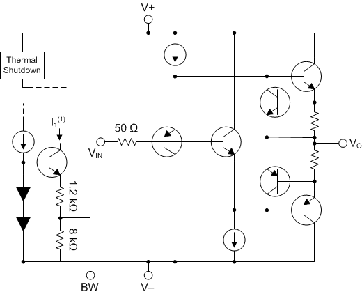
Stage currents are set by I1.