SWRS037B January 2006 – March 2015 CC1150
PRODUCTION DATA.
- 1Device Overview
- 2Revision History
- 3Terminal Configuration and Functions
-
4Specifications
- 4.1 Absolute Maximum Ratings
- 4.2 ESD Ratings
- 4.3 Recommended Operating Conditions
- 4.4 General Characteristics
- 4.5 Current Consumption
- 4.6 RF Transmit
- 4.7 Crystal Oscillator
- 4.8 Frequency Synthesizer Characteristics
- 4.9 Analog Temperature Sensor
- 4.10 DC Characteristics
- 4.11 Power-On Reset
- 4.12 Thermal Resistance Characteristics for VQFNP Package
-
5Detailed Description
- 5.1 Overview
- 5.2 Functional Block Diagram
- 5.3 Configuration Overview
- 5.4 Configuration Software
- 5.5 4-wire Serial Configuration and Data Interface
- 5.6 Microcontroller Interface and Pin Configuration
- 5.7 Data Rate Programming
- 5.8 Packet Handling Hardware Support
- 5.9 Modulation Formats
- 5.10 Forward Error Correction with Interleaving
- 5.11 Radio Control
- 5.12 Data FIFO
- 5.13 Frequency Programming
- 5.14 VCO
- 5.15 Voltage Regulators
- 5.16 Output Power Programming
- 5.17 General Purpose and Test Output Control Pins
- 5.18 Asynchronous and Synchronous Serial Operation
- 5.19 System Considerations and Guidelines
- 5.20 Memory
- 6Applications, Implementation, and Layout
- 7Device and Documentation Support
- 8Mechanical Packaging and Orderable Information
Package Options
Mechanical Data (Package|Pins)
- RGV|16
Thermal pad, mechanical data (Package|Pins)
- RGV|16
Orderable Information
1 Device Overview
1.1 Features
- Small Size
- QLP 4-mm × 4-mm Package, 16 Pins
- True Single Chip UHF RF Transmitter
- Frequency Bands
- 300 to 348 MHz
- 400 to 464 MHz
- 800 to 928 MHz
- Programmable Data Rate Up to 500 kBaud
- Low Current Consumption
- Programmable Output Power Up to +10 dBm for All Supported Frequencies
- Programmable Baseband Modulator
- Ideal For Multi-channel Operation
- Very Few External Components
- Completely On-chip Frequency Synthesizer
- No External Filters Needed
- Configurable Packet Handling Hardware
- Suitable for Frequency Hopping Systems Due to a Fast Settling Frequency Synthesizer
- Optional Forward Error Correction with Interleaving
- 64-byte TX Data FIFO
- Suited for Systems Compliant with EN 300 220 and FCC CFR Part 15
- Many Powerful Digital Features Allow a High-performance RF system to be made Using an Inexpensive Microcontroller
- Efficient SPI interface: All Registers Can be Programmed With One "Burst" Transfer
- Integrated Analog Temperature Sensor
- Lead-free “Green” Package
- Flexible Support for Packet Oriented Systems
- On-chip Support for Sync-Word Insertion, Flexible Packet Length and Automatic CRC Handling
- OOK and Flexible ASK Shaping Supported
- 2-FSK, GFSK and MSK Supported
- Optional Automatic Whitening of Data
- Support for Asynchronous Transparent Transmit Mode for Backwards Compatibility with Existing Radio Communication Protocols
1.2 Applications
- Ultra-low Power UHF Wireless Transmitters
- Operating in the 315-, 433-, 868-, and 915-MHz ISM/SRD bands
- AMR – Automatic Meter Reading
- Consumer Electronics
- RKE – Remote Keyless Entry
- Low Power Telemetry
- Home and Building Automation
- Wireless Alarm and Security Systems
- Industrial Monitoring and Control
- Wireless Sensor Networks
1.3 Description
The CC1150 is a true single-chip UHF transmitter designed for very low power wireless applications. The circuit is mainly intended for the ISM (Industrial, Scientific and Medical) and SRD (Short Range Device) frequency bands at 315-, 433-, 868-, and 915-MHz, but can easily be programmed for operation at other frequencies in the 300 to 348 MHz, 400 to 464 MHz and 800 to 928 MHz bands.
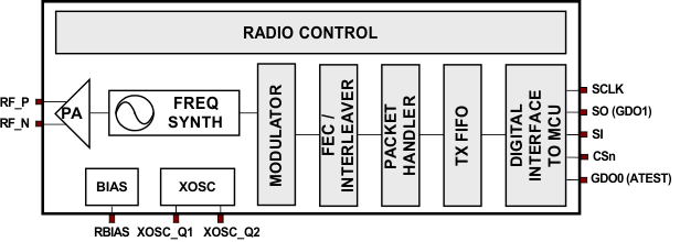
The RF transmitter is integrated with a highly configurable baseband modulator. The modulator supports various modulation formats and has a configurable data rate up to 500 kBaud. The CC1150 device provides extensive hardware support for packet handling, data buffering and burst transmissions.
The main operating parameters and the 64-byte transmit FIFO of CC1150 can be controlled via an SPI interface. In a typical system, the CC1150 device will be used together with a microcontroller and a few additional passive components.
CC1150 is part of the SmartRF™ technology platform based on 0.18-μm CMOS technology from Texas Instruments.
1.4 Functional Block Diagram
