SWRS192F July 2018 – February 2021 CC1352P
PRODUCTION DATA
- 1 Features
- 2 Applications
- 3 Description
- 4 Functional Block Diagram
- 5 Revision History
- 6 Device Comparison
- 7 Terminal Configuration and Functions
-
8 Specifications
- 8.1 Absolute Maximum Ratings
- 8.2 ESD Ratings
- 8.3 Recommended Operating Conditions
- 8.4 Power Supply and Modules
- 8.5 Power Consumption - Power Modes
- 8.6 Power Consumption - Radio Modes
- 8.7 Nonvolatile (Flash) Memory Characteristics
- 8.8 Thermal Resistance Characteristics
- 8.9 RF Frequency Bands
- 8.10 861 MHz to 1054 MHz - Receive (RX)
- 8.11 861 MHz to 1054 MHz - Transmit (TX)
- 8.12 861 MHz to 1054 MHz - PLL Phase Noise Wideband Mode
- 8.13 861 MHz to 1054 MHz - PLL Phase Noise Narrowband Mode
- 8.14 359 MHz to 527 MHz - Receive (RX)
- 8.15 359 MHz to 527 MHz - Transmit (TX)
- 8.16 359 MHz to 527 MHz - PLL Phase Noise
- 8.17 143 MHz to 176 MHz - Receive (RX)
- 8.18 143 MHz to 176 MHz - Transmit (TX)
- 8.19 143 MHz to 176 MHz - PLL Phase Noise
- 8.20 Bluetooth Low Energy - Receive (RX)
- 8.21 Bluetooth Low Energy - Transmit (TX)
- 8.22 Zigbee and Thread - IEEE 802.15.4-2006 2.4 GHz (OQPSK DSSS1:8, 250 kbps) - RX
- 8.23 Zigbee and Thread - IEEE 802.15.4-2006 2.4 GHz (OQPSK DSSS1:8, 250 kbps) - TX
- 8.24 Timing and Switching Characteristics
- 8.25 Peripheral Characteristics
- 8.26 Typical Characteristics
- 9 Detailed Description
- 10Application, Implementation, and Layout
- 11Device and Documentation Support
- 12Mechanical, Packaging, and Orderable Information
Package Options
Refer to the PDF data sheet for device specific package drawings
Mechanical Data (Package|Pins)
- RGZ|48
Thermal pad, mechanical data (Package|Pins)
- RGZ|48
Orderable Information
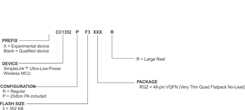
11.1 Device Nomenclature
To designate the stages in the product development cycle, TI assigns prefixes to all part numbers and/or date-code. Each device has one of three prefixes/identifications: X, P, or null (no prefix) (for example, XCC1352P is in preview; therefore, an X prefix/identification is assigned).
Device development evolutionary flow:
- XExperimental device that is not necessarily representative of the final device's electrical specifications and may not use production assembly flow.
- PPrototype device that is not necessarily the final silicon die and may not necessarily meet final electrical specifications.
- nullProduction version of the silicon die that is fully qualified.
Production devices have been characterized fully, and the quality and reliability of the device have been demonstrated fully. TI's standard warranty applies.
Predictions show that prototype devices (X or P) have a greater failure rate than the standard production devices. Texas Instruments recommends that these devices not be used in any production system because their expected end-use failure rate still is undefined. Only qualified production devices are to be used.
TI device nomenclature also includes a suffix with the device family name. This suffix indicates the package type (for example, RGZ).
For orderable part numbers of CC1352P devices in the RGZ (7-mm x 7-mm) package type, see the Package Option Addendum of this document, the Device Information in Section 3, the TI website (www.ti.com), or contact your TI sales representative.
 Figure 11-1 Device Nomenclature