SWRS205E March   2017  – May 2021 CC3120MOD

PRODUCTION DATA  

  1. Features
  2. Applications
  3. Description
  4. Functional Block Diagrams
  5. Revision History
  6. Device Comparison
    1. 6.1 Related Products
  7. Terminal Configuration and Functions
    1. 7.1 CC3120MOD Pin Diagram
    2. 7.2 Pin Attributes
      1.      11
    3. 7.3 Connections for Unused Pins
  8. Specifications
    1. 8.1  Absolute Maximum Ratings
    2. 8.2  ESD Ratings
    3. 8.3  Recommended Operating Conditions
    4. 8.4  Current Consumption Summary
    5. 8.5  TX Power and IBAT versus TX Power Level Settings
    6. 8.6  Brownout and Blackout Conditions
    7. 8.7  Electrical Characteristics
    8. 8.8  WLAN Receiver Characteristics
    9. 8.9  WLAN Transmitter Characteristics
    10. 8.10 Reset Requirement
    11. 8.11 Thermal Resistance Characteristics for MOB Package
    12. 8.12 Timing and Switching Characteristics
      1. 8.12.1 Power-Up Sequencing
      2. 8.12.2 Power-Down Sequencing
      3. 8.12.3 Device Reset
      4. 8.12.4 Wakeup From HIBERNATE Mode Timing
    13. 8.13 External Interfaces
      1. 8.13.1 SPI Host Interface
      2. 8.13.2 Host UART Interface
        1. 8.13.2.1 5-Wire UART Topology
        2. 8.13.2.2 4-Wire UART Topology
        3. 8.13.2.3 3-Wire UART Topology
      3. 8.13.3 External Flash Interface
  9. Detailed Description
    1. 9.1 Overview
    2. 9.2 Module Features
      1. 9.2.1 WLAN
      2. 9.2.2 Network Stack
        1. 9.2.2.1 Security
      3. 9.2.3 Host Interface and Driver
      4. 9.2.4 System
    3. 9.3 Power-Management Subsystem
      1. 9.3.1 VBAT Wide-Voltage Connection
    4. 9.4 Low-Power Operating Modes
      1. 9.4.1 Low-Power Deep Sleep
      2. 9.4.2 Hibernate
      3. 9.4.3 Shutdown
    5. 9.5 Restoring Factory Default Configuration
    6. 9.6 Device Certification and Qualification
      1. 9.6.1 FCC Certification and Statement
      2. 9.6.2 Industry Canada (IC) Certification and Statement
      3. 9.6.3 ETSI/CE Certification
      4. 9.6.4 Japan MIC Certification
      5. 9.6.5 SRRC Certification and Statement
    7. 9.7 Module Markings
    8. 9.8 End Product Labeling
    9. 9.9 Manual Information to the End User
  10. 10Applications, Implementation, and Layout
    1. 10.1 Application Information
      1. 10.1.1 Typical Application
      2. 10.1.2 Power Supply Decoupling and Bulk Capacitors
      3. 10.1.3 Reset
      4. 10.1.4 Unused Pins
    2. 10.2 PCB Layout Guidelines
      1. 10.2.1 General Layout Recommendations
      2. 10.2.2 RF Layout Recommendations
      3. 10.2.3 Antenna Placement and Routing
      4. 10.2.4 Transmission Line Considerations
  11. 11Environmental Requirements and Specifications
    1. 11.1 Temperature
      1. 11.1.1 PCB Bending
    2. 11.2 Handling Environment
      1. 11.2.1 Terminals
      2. 11.2.2 Falling
    3. 11.3 Storage Condition
      1. 11.3.1 Moisture Barrier Bag Before Opened
      2. 11.3.2 Moisture Barrier Bag Open
    4. 11.4 Baking Conditions
    5. 11.5 Soldering and Reflow Condition
  12. 12Device and Documentation Support
    1. 12.1 Device Nomenclature
    2. 12.2 Development Tools and Software
    3. 12.3 Firmware Updates
    4. 12.4 Documentation Support
    5. 12.5 Trademarks
    6. 12.6 Electrostatic Discharge Caution
    7. 12.7 Glossary
  13. 13Mechanical, Packaging, and Orderable Information
    1. 13.1 Mechanical, Land, and Solder Paste Drawings
    2. 13.2 Package Option Addendum
      1. 13.2.1 Packaging Information
    3. 13.3 Tape and Reel Information
      1. 13.3.1 Tape and Reel Specification

Refer to the PDF data sheet for device specific package drawings

Mechanical Data (Package|Pins)
  • MOB|63
Thermal pad, mechanical data (Package|Pins)

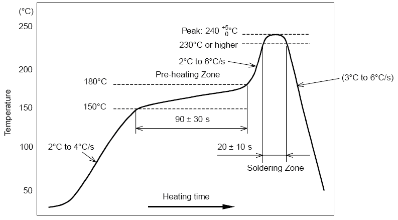
Soldering and Reflow Condition

  • Heating method: Conventional convection or IR convection
  • Temperature measurement: Thermocouple d = 0.1 mm to 0.2 mm CA (K) or CC (T) at soldering portion or equivalent method
  • Solder paste composition: Sn/3.0 Ag/0.5 Cu
  • Allowable reflow soldering times: 2 times based on the reflow soldering profile
    (see Figure 11-1)
  • Temperature profile: Reflow soldering will be done according to the temperature profile (see
    Figure 11-1)
  • Peak temp: 245°C
GUID-49123E94-0B33-466E-8907-510762CF9E71-low.png Figure 11-1 Temperature Profile for Evaluation of Solder Heat Resistance of a Component (at Solder Joint)
Note:

TI does not recommend the use of conformal coating or similar material on the SimpleLink module. This coating can lead to localized stress on the WCSP solder connections inside the module and impact the device reliability. Use caution during the module assembly process to the final PCB to avoid the presence of foreign material inside the module.