SWRS205E March   2017  – May 2021 CC3120MOD

PRODUCTION DATA  

  1. Features
  2. Applications
  3. Description
  4. Functional Block Diagrams
  5. Revision History
  6. Device Comparison
    1. 6.1 Related Products
  7. Terminal Configuration and Functions
    1. 7.1 CC3120MOD Pin Diagram
    2. 7.2 Pin Attributes
      1.      11
    3. 7.3 Connections for Unused Pins
  8. Specifications
    1. 8.1  Absolute Maximum Ratings
    2. 8.2  ESD Ratings
    3. 8.3  Recommended Operating Conditions
    4. 8.4  Current Consumption Summary
    5. 8.5  TX Power and IBAT versus TX Power Level Settings
    6. 8.6  Brownout and Blackout Conditions
    7. 8.7  Electrical Characteristics
    8. 8.8  WLAN Receiver Characteristics
    9. 8.9  WLAN Transmitter Characteristics
    10. 8.10 Reset Requirement
    11. 8.11 Thermal Resistance Characteristics for MOB Package
    12. 8.12 Timing and Switching Characteristics
      1. 8.12.1 Power-Up Sequencing
      2. 8.12.2 Power-Down Sequencing
      3. 8.12.3 Device Reset
      4. 8.12.4 Wakeup From HIBERNATE Mode Timing
    13. 8.13 External Interfaces
      1. 8.13.1 SPI Host Interface
      2. 8.13.2 Host UART Interface
        1. 8.13.2.1 5-Wire UART Topology
        2. 8.13.2.2 4-Wire UART Topology
        3. 8.13.2.3 3-Wire UART Topology
      3. 8.13.3 External Flash Interface
  9. Detailed Description
    1. 9.1 Overview
    2. 9.2 Module Features
      1. 9.2.1 WLAN
      2. 9.2.2 Network Stack
        1. 9.2.2.1 Security
      3. 9.2.3 Host Interface and Driver
      4. 9.2.4 System
    3. 9.3 Power-Management Subsystem
      1. 9.3.1 VBAT Wide-Voltage Connection
    4. 9.4 Low-Power Operating Modes
      1. 9.4.1 Low-Power Deep Sleep
      2. 9.4.2 Hibernate
      3. 9.4.3 Shutdown
    5. 9.5 Restoring Factory Default Configuration
    6. 9.6 Device Certification and Qualification
      1. 9.6.1 FCC Certification and Statement
      2. 9.6.2 Industry Canada (IC) Certification and Statement
      3. 9.6.3 ETSI/CE Certification
      4. 9.6.4 Japan MIC Certification
      5. 9.6.5 SRRC Certification and Statement
    7. 9.7 Module Markings
    8. 9.8 End Product Labeling
    9. 9.9 Manual Information to the End User
  10. 10Applications, Implementation, and Layout
    1. 10.1 Application Information
      1. 10.1.1 Typical Application
      2. 10.1.2 Power Supply Decoupling and Bulk Capacitors
      3. 10.1.3 Reset
      4. 10.1.4 Unused Pins
    2. 10.2 PCB Layout Guidelines
      1. 10.2.1 General Layout Recommendations
      2. 10.2.2 RF Layout Recommendations
      3. 10.2.3 Antenna Placement and Routing
      4. 10.2.4 Transmission Line Considerations
  11. 11Environmental Requirements and Specifications
    1. 11.1 Temperature
      1. 11.1.1 PCB Bending
    2. 11.2 Handling Environment
      1. 11.2.1 Terminals
      2. 11.2.2 Falling
    3. 11.3 Storage Condition
      1. 11.3.1 Moisture Barrier Bag Before Opened
      2. 11.3.2 Moisture Barrier Bag Open
    4. 11.4 Baking Conditions
    5. 11.5 Soldering and Reflow Condition
  12. 12Device and Documentation Support
    1. 12.1 Device Nomenclature
    2. 12.2 Development Tools and Software
    3. 12.3 Firmware Updates
    4. 12.4 Documentation Support
    5. 12.5 Trademarks
    6. 12.6 Electrostatic Discharge Caution
    7. 12.7 Glossary
  13. 13Mechanical, Packaging, and Orderable Information
    1. 13.1 Mechanical, Land, and Solder Paste Drawings
    2. 13.2 Package Option Addendum
      1. 13.2.1 Packaging Information
    3. 13.3 Tape and Reel Information
      1. 13.3.1 Tape and Reel Specification

Refer to the PDF data sheet for device specific package drawings

Mechanical Data (Package|Pins)
  • MOB|63
Thermal pad, mechanical data (Package|Pins)

Module Markings

Figure 9-1 shows the markings for the SimpleLink CC3120 Module.(1)
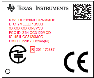
GUID-C2D6D3B5-579B-47F4-9F4F-62D831E4B49C-low.gifFigure 9-1 SimpleLink™ CC3120 Module Markings

Table 9-3 lists the SimpleLink module markings.

Table 9-3 Marking Descriptions
MARKINGDESCRIPTION
CC3120MODRNMMOBModel
YMLLLLP SSSSLTC (lot trace code):
  • Y = Year
  • M = Month
  • LLLL = Assembly lot code
  • P = Reserved for internal use
  • SSSS = Serial number
XXXXXXXXXX-VVSSTI internal use only
Z64-CC3120MODFCC ID: single modular FCC grant ID
451I-CC3120MODIC: single modular IC grant ID
2017DJ2946(M)CMIIT: limited modular SRRC grant ID
GUID-FD0CAC28-2496-4B5E-9719-820EA8039A91-low.gifMIC compliance mark
GUID-0898B29E-DC05-4723-B726-A69ED05990D3-low.gifMIC ID: modular MIC grant ID
CECE compliance mark


Drawings are representative. Content or placement may vary from what is illustrated.