SWAS035C September   2016  – May 2021 CC3220R , CC3220S , CC3220SF

PRODUCTION DATA  

  1. Features
  2. Applications
  3. Description
  4. Functional Block Diagrams
  5. Revision History
  6. Device Comparison
    1. 6.1 Related Products
  7. Terminal Configuration and Functions
    1. 7.1 Pin Diagram
    2. 7.2 Pin Attributes and Pin Multiplexing
      1. 7.2.1 Pin Descriptions
    3. 7.3 Signal Descriptions
      1. 7.3.1 Signal Descriptions
    4. 7.4 Pin Multiplexing
    5. 7.5 Drive Strength and Reset States for Analog and Digital Multiplexed Pins
    6. 7.6 Pad State After Application of Power to Chip But Before Reset Release
    7. 7.7 Connections for Unused Pins
  8. Specifications
    1. 8.1  Absolute Maximum Ratings
    2. 8.2  ESD Ratings
    3. 8.3  Power-On Hours (POH)
    4. 8.4  Recommended Operating Conditions
    5. 8.5  Current Consumption Summary (CC3220R, CC3220S)
    6. 8.6  Current Consumption Summary (CC3220SF)
    7. 8.7  TX Power and IBAT versus TX Power Level Settings
    8. 8.8  Brownout and Blackout Conditions
    9. 8.9  Electrical Characteristics (3.3 V, 25°C)
    10. 8.10 WLAN Receiver Characteristics
    11. 8.11 WLAN Transmitter Characteristics
    12. 8.12 WLAN Filter Requirements
      1. 8.12.1 WLAN Filter Requirements
    13. 8.13 Thermal Resistance Characteristics
      1. 8.13.1 Thermal Resistance Characteristics for RGK Package
    14. 8.14 Timing and Switching Characteristics
      1. 8.14.1 Power Supply Sequencing
      2. 8.14.2 Device Reset
      3. 8.14.3 Reset Timing
        1. 8.14.3.1 nRESET (32-kHz Crystal)
        2. 8.14.3.2 First-Time Power-Up and Reset Removal Timing Requirements (32-kHz Crystal)
        3. 8.14.3.3 nRESET (External 32-kHz)
          1. 8.14.3.3.1 First-Time Power-Up and Reset Removal Timing Requirements (External 32-kHz)
      4. 8.14.4 Wakeup From HIBERNATE Mode
      5. 8.14.5 Clock Specifications
        1. 8.14.5.1 Slow Clock Using Internal Oscillator
          1. 8.14.5.1.1 RTC Crystal Requirements
        2. 8.14.5.2 Slow Clock Using an External Clock
          1. 8.14.5.2.1 External RTC Digital Clock Requirements
        3. 8.14.5.3 Fast Clock (Fref) Using an External Crystal
          1. 8.14.5.3.1 WLAN Fast-Clock Crystal Requirements
        4. 8.14.5.4 Fast Clock (Fref) Using an External Oscillator
          1. 8.14.5.4.1 External Fref Clock Requirements (–40°C to +85°C)
      6. 8.14.6 Peripherals Timing
        1. 8.14.6.1  SPI
          1. 8.14.6.1.1 SPI Master
            1. 8.14.6.1.1.1 SPI Master Timing Parameters
          2. 8.14.6.1.2 SPI Slave
            1. 8.14.6.1.2.1 SPI Slave Timing Parameters
        2. 8.14.6.2  I2S
          1. 8.14.6.2.1 I2S Transmit Mode
            1. 8.14.6.2.1.1 I2S Transmit Mode Timing Parameters
          2. 8.14.6.2.2 I2S Receive Mode
            1. 8.14.6.2.2.1 I2S Receive Mode Timing Parameters
        3. 8.14.6.3  GPIOs
          1. 8.14.6.3.1 GPIO Output Transition Time Parameters (Vsupply = 3.3 V)
            1. 8.14.6.3.1.1 GPIO Output Transition Times (Vsupply = 3.3 V) (1) (1)
          2. 8.14.6.3.2 GPIO Output Transition Time Parameters (Vsupply = 1.85 V)
            1. 8.14.6.3.2.1 GPIO Output Transition Times (Vsupply = 1.85 V) (1) (1)
          3. 8.14.6.3.3 GPIO Input Transition Time Parameters
            1. 8.14.6.3.3.1 GPIO Input Transition Time Parameters'
        4. 8.14.6.4  I2C
          1. 8.14.6.4.1 I2C Timing Parameters (1)
        5. 8.14.6.5  IEEE 1149.1 JTAG
          1. 8.14.6.5.1 JTAG Timing Parameters
        6. 8.14.6.6  ADC
          1. 8.14.6.6.1 ADC Electrical Specifications
        7. 8.14.6.7  Camera Parallel Port
          1. 8.14.6.7.1 Camera Parallel Port Timing Parameters
        8. 8.14.6.8  UART
        9. 8.14.6.9  SD Host
        10. 8.14.6.10 Timers
  9. Detailed Description
    1. 9.1 Arm® Cortex®-M4 Processor Core Subsystem
    2. 9.2 Wi-Fi Network Processor Subsystem
      1. 9.2.1 WLAN
      2. 9.2.2 Network Stack
    3. 9.3 Security
    4. 9.4 Power-Management Subsystem
      1. 9.4.1 VBAT Wide-Voltage Connection
      2. 9.4.2 Preregulated 1.85-V Connection
    5. 9.5 Low-Power Operating Mode
    6. 9.6 Memory
      1. 9.6.1 External Memory Requirements
      2. 9.6.2 Internal Memory
        1. 9.6.2.1 SRAM
        2. 9.6.2.2 ROM
        3. 9.6.2.3 Flash Memory
        4. 9.6.2.4 Memory Map
    7. 9.7 Restoring Factory Default Configuration
    8. 9.8 Boot Modes
      1. 9.8.1 Boot Mode List
  10. 10Applications, Implementation, and Layout
    1. 10.1 Application Information
      1. 10.1.1 Typical Application —CC3220x Wide-Voltage Mode
      2. 10.1.2 Typical Application Schematic—CC3220x Preregulated, 1.85-V Mode
    2. 10.2 PCB Layout Guidelines
      1. 10.2.1 General PCB Guidelines
      2. 10.2.2 Power Layout and Routing
        1. 10.2.2.1 Design Considerations
      3. 10.2.3 Clock Interfaces
      4. 10.2.4 Digital Input and Output
      5. 10.2.5 RF Interface
  11. 11Device and Documentation Support
    1. 11.1 Development Tools and Software
    2. 11.2 Firmware Updates
    3. 11.3 Device Nomenclature
    4. 11.4 Documentation Support
    5. 11.5 Support Resources
    6. 11.6 Trademarks
    7. 11.7 Electrostatic Discharge Caution
    8. 11.8 Export Control Notice
    9. 11.9 Glossary
  12. 12Mechanical, Packaging, and Orderable Information
    1. 12.1 Packaging Information

Package Options

Mechanical Data (Package|Pins)
Thermal pad, mechanical data (Package|Pins)
Orderable Information

TX Power and IBAT versus TX Power Level Settings

Figure 8-1, Figure 8-2, and Figure 8-3 show TX Power and IBAT versus TX power level settings for the CC3220R and CC3220S devices at modulations of 1 DSSS, 6 OFDM, and 54 OFDM, respectively. For the CC3220SF device, the IBAT current has an increase of approximately 10 mA to 15 mA depending on the transmitted rate. The TX power level will remain the same.

In Figure 8-1, the area enclosed in the circle represents a significant reduction in current during transition from TX power level 3 to level 4. In the case of lower range requirements (14-dBm output power), TI recommends using TX power level 4 to reduce the current.
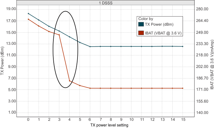
GUID-0230D56F-A13D-4412-9BE2-9F195B779F71-low.gifFigure 8-1 TX Power and IBAT vs TX Power Level Settings (1 DSSS)
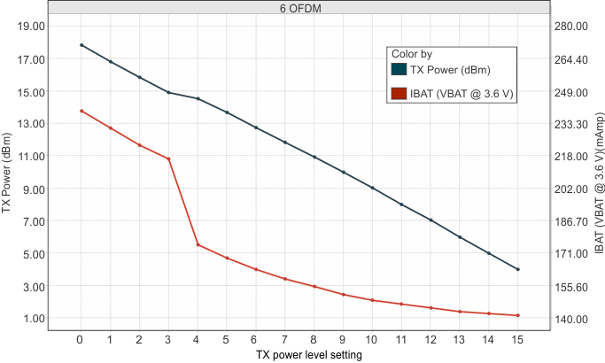
GUID-0CEB5A6E-C13C-4469-97FB-E4ED21B608B6-low.gifFigure 8-2 TX Power and IBAT vs TX Power Level Settings (6 OFDM)
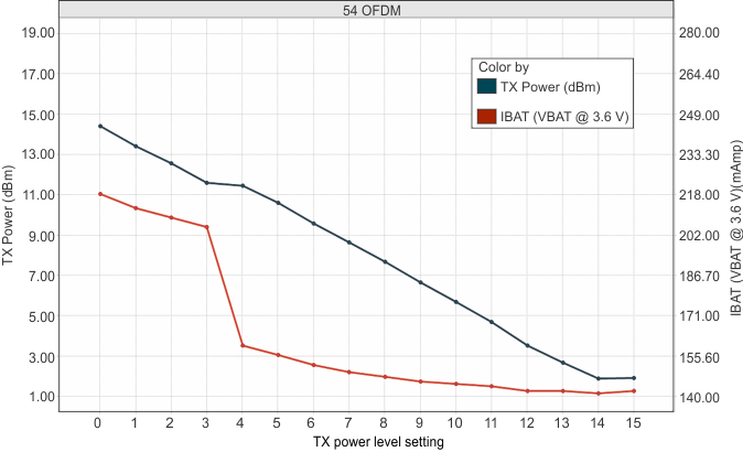
GUID-6CAA94A3-A024-46E1-BD21-DDA823B9B121-low.gifFigure 8-3 TX Power and IBAT vs TX Power Level Settings (54 OFDM)