SCHS047L august 1998 – september 2023 CD4051B , CD4052B , CD4053B
PRODUCTION DATA
- 1
- 1 Features
- 2 Applications
- 3 Description
- 4 Revision History
- 5 Pin Configuration and Functions
- 6 Specifications
- 7 Parameter Measurement Information
- 8 Detailed Description
- 9 Application and Implementation
- 10Device and Documentation Support
- 11Mechanical, Packaging, and Orderable Information
Package Options
Mechanical Data (Package|Pins)
Thermal pad, mechanical data (Package|Pins)
- D|16
Orderable Information
3 Description
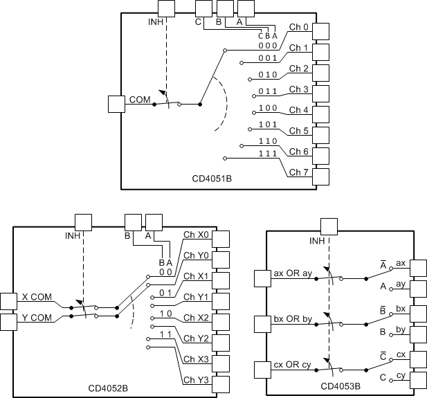
The CD405xB analog multiplexers and demultiplexers are digitally-controlled analog switches having low ON impedance and very low OFF leakage current. These multiplexer circuits dissipate extremely low quiescent power over the full VDD – VSS and VDD – VEE supply-voltage ranges, independent of the logic state of the control signals.
Package
Information
| PART NUMBER | PACKAGE(1) | PACKAGE SIZE(2) |
|---|---|---|
| CD405xB | J (CDIP, 16) | 19.50 mm × 6.92 mm |
| N (PDIP, 16) | 19.3 mm × 9.4 mm | |
| D (SOIC, 16) | 9.9 mm × 6 mm | |
| NS (SOP, 16) | 10.2 mm × 7.8 mm | |
| PW (TSSOP, 16) | 5 mm × 6.4 mm |
(1) For all available packages, see the orderable addendum at the end of the data
sheet.
(2) The package size (length × width) is a nominal value
and includes pins, where applicable.
 Functional Diagrams of CD405xB