SNAS818B July 2021 – May 2022 CDCDB800
PRODUCTION DATA
- 1 Features
- 2 Applications
- 3 Description
- 4 Revision History
- 5 Pin Configuration and Functions
- 6 Specifications
- 7 Parameter Measurement Information
- 8 Detailed Description
- 9 Application and Implementation
- 10Power Supply Recommendations
- 11Layout
- 12Device and Documentation Support
- 13Mechanical, Packaging, and Orderable Information
Package Options
Mechanical Data (Package|Pins)
- RSL|48
Thermal pad, mechanical data (Package|Pins)
- RSL|48
Orderable Information
8.4.1 CKPWRGD_PD# Function
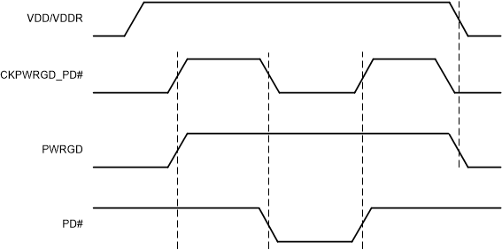
The CKPWRGD_PD# pin is used to set two state variables inside of the device: PWRGD and PD#. The PWRGD and PD# variables control which functions of the device are active at any time, as well as the state of the input and output pins.
The PWRGD and PD# states are multiplexed on the CKPWRGD_PD# pin. CKPWRGD_PD# must remain below VOL and not exceed VDDR + 0.3 V until VDD and VDDR are present and within the recommended operating conditions. After CKPWRGD_PD# is set high, a valid CLKIN must be present to use PD#.
The first rising edge of the CKPWRGD_PD# pin sets PWRGD = 1. After PWRGD is set to 1, the CKPWRGD_PD# pin is used to assert PD# mode only. PWRGD variable will only be cleared to 0 with the removal of VDD and VDDR.
 Figure 8-1 PWRGD and PD# State Changes