SLPS448F July 2013 – January 2022 CSD13381F4
PRODUCTION DATA
- 1Features
- 2Applications
- 3Description
- 4Revision History
- 5Specifications
- 6Device and Documentation Support
- 7Mechanical, Packaging, and Orderable Information
Package Options
Refer to the PDF data sheet for device specific package drawings
Mechanical Data (Package|Pins)
- YJC|3
Thermal pad, mechanical data (Package|Pins)
Orderable Information
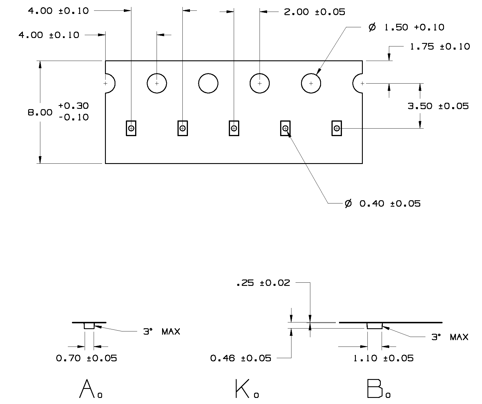
7.4 CSD13381F4 Embossed Carrier Tape Dimensions
Pin 1 is oriented in the top-right quadrant of the tape enclosure (quadrant 2), closest to the carrier tape sprocket holes.