SLPS482B December 2013 – January 2015 CSD19533KCS
PRODUCTION DATA.
- 1Features
- 2Applications
- 3Description
- 4Revision History
- 5Specifications
- 6Device and Documentation Support
- 7Mechanical, Packaging, and Orderable Information
Package Options
Refer to the PDF data sheet for device specific package drawings
Mechanical Data (Package|Pins)
- KCS|3
Thermal pad, mechanical data (Package|Pins)
Orderable Information
5 Specifications
5.1 Electrical Characteristics
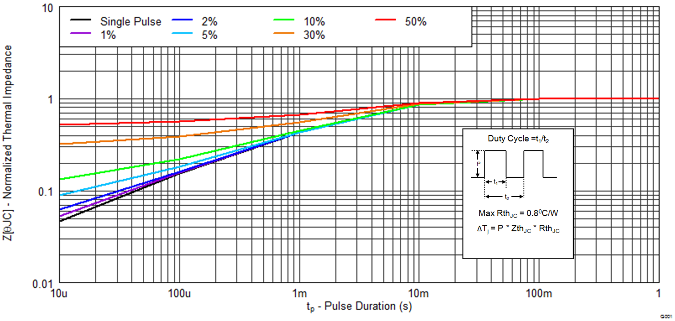
(TA = 25°C unless otherwise stated)5.2 Thermal Information
(TA = 25°C unless otherwise stated)| THERMAL METRIC | MIN | TYP | MAX | UNIT | |
|---|---|---|---|---|---|
| RθJC | Junction-to-Case Thermal Resistance | 0.8 | °C/W | ||
| RθJA | Junction-to-Ambient Thermal Resistance | 62 | |||
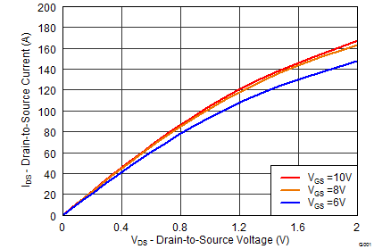
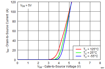
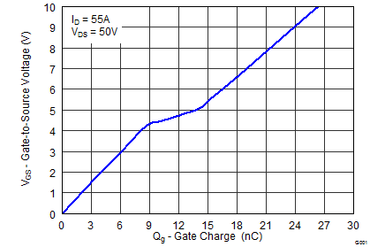
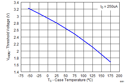
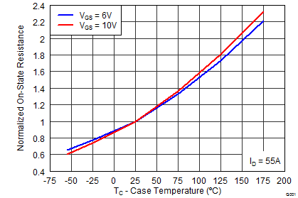
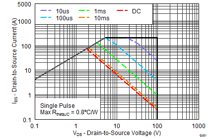
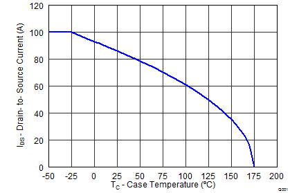
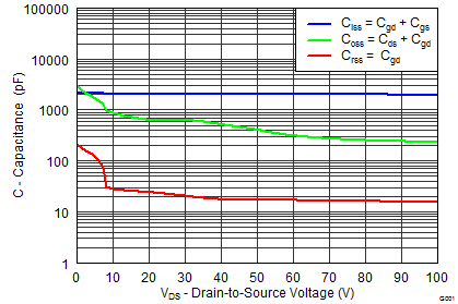
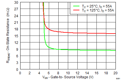
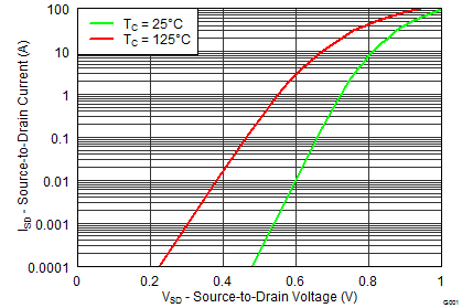
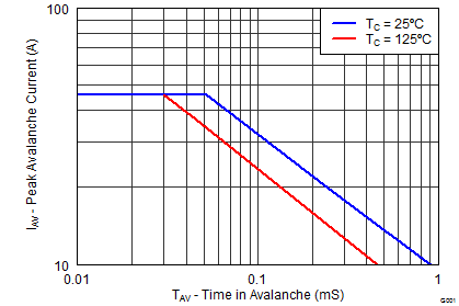
5.3 Typical MOSFET Characteristics
(TA = 25°C unless otherwise stated)