SLPS671A June 2017 – January 2018 CSD95495QVM
PRODUCTION DATA.
- 1Features
- 2Applications
- 3Description
- 4Revision History
- 5Pin Configuration and Functions
- 6Specifications
- 7Application Schematic
- 8Device and Documentation Support
- 9Mechanical, Packaging, and Orderable Information
Package Options
Mechanical Data (Package|Pins)
- DMH|18
Thermal pad, mechanical data (Package|Pins)
Orderable Information
1 Features
- 50-A Continuous Operating Current Capability
- Over 93.5% System Efficiency at 25 A
- High-Frequency Operation (up to 1.25 MHz)
- Diode Emulation Function
- Temperature Compensated Bi-Directional Current Sense
- Analog Temperature Output
- Fault Monitoring
- 3.3-V and 5-V PWM Signal Compatible
- Tri-State PWM Input
- Integrated Bootstrap Switch
- Optimized Dead Time for Shoot-Through Protection
- High-Density VSON 4-mm × 5-mm Footprint
- Ultra-Low-Inductance Package
- System Optimized PCB Footprint
- RoHS Compliant – Lead-Free Terminal Plating
- Halogen Free
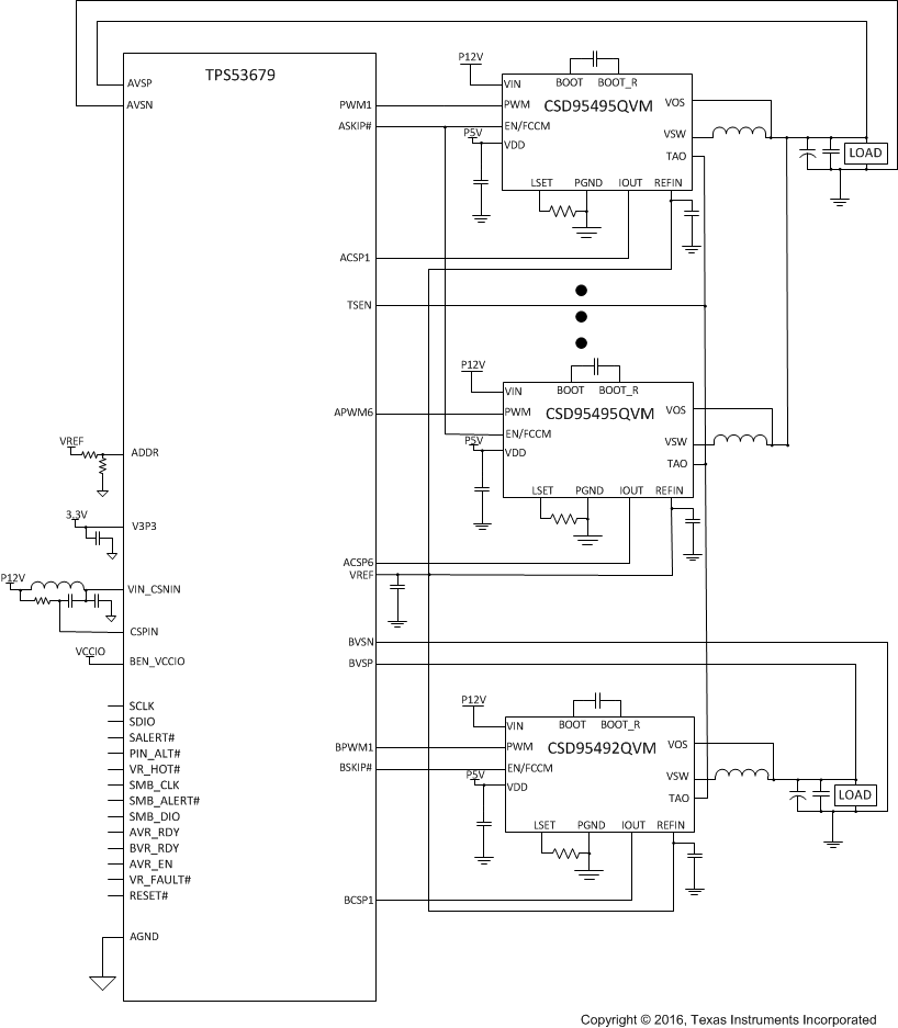
Application Diagram
