SNVS801B April 2012 – January 2016 DAC101C081 , DAC101C081Q , DAC101C085
PRODUCTION DATA.
- 1 Features
- 2 Applications
- 3 Description
- 4 Revision History
- 5 Description (continued)
- 6 Device Comparison Table
- 7 Pin Configuration and Functions
- 8 Specifications
- 9 Detailed Description
- 10Application and Implementation
- 11Power Supply Recommendations
- 12Layout
- 13Device and Documentation Support
- 14Mechanical, Packaging, and Orderable Information
Package Options
Mechanical Data (Package|Pins)
Thermal pad, mechanical data (Package|Pins)
Orderable Information
12 Layout
12.1 Layout Guidelines
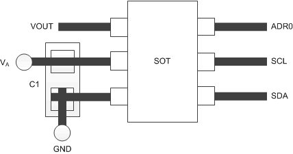
For best accuracy and minimum noise, the printed circuit board containing the DAC101C081 requires separate analog and digital areas. The areas are defined by the locations of the analog and digital power planes. Both of these planes should be located on the same board layer. There should be a single ground plane. A single ground plane is preferred if digital return current does not flow through the analog ground area. Frequently a single ground plane design will use a fencing technique to prevent the mixing of analog and digital ground current. Separate ground planes should only be utilized when the fencing technique is inadequate. The separate ground planes must be connected in one place, preferably near the DAC101C081. Special care is required to ensure that digital signals with fast edge rates do not pass over split ground planes. They must always have a continuous return path below their traces.
The DAC101C081 power supply should be bypassed with a 4.7-µF and a 0.1-µF capacitor as close as possible to the device with the 0.1 µF right at the device supply pin. The 4.7-µF capacitor should be a tantalum type and the 0.1-µF capacitor should be a low ESL, low ESR type. The power supply for the DAC101C081 should only be used for analog circuits.
Avoid crossover of analog and digital signals and keep the clock and data lines on the component side of the board. These clock and data lines require controlled impedances.
12.2 Layout Example
 Figure 35. Layout Example