SLASEL0B October 2019 – June 2020 DAC11001A , DAC81001 , DAC91001
PRODUCTION DATA.
- 1 Features
- 2 Applications
- 3 Description
- 4 Revision History
- 5 Device Comparison Table
- 6 Pin Configuration and Functions
-
7 Specifications
- 7.1 Absolute Maximum Ratings
- 7.2 ESD Ratings
- 7.3 Recommended Operating Conditions
- 7.4 Thermal Information Package
- 7.5 Electrical Characteristics
- Table 1. Timing Requirements: Write, 4.5 V ≤ DVDD ≤ 5.5 V
- Table 2. Timing Requirements: Write, 2.7 V ≤ DVDD < 4.5 V
- Table 3. Timing Requirements: Read and Daisy-Chain Write, 4.5 V ≤ DVDD ≤ 5.5 V
- Table 4. Timing Requirements: Read and Daisy-Chain Write, 2.7 V ≤ DVDD < 4.5 V
- 7.6 Typical Characteristics
-
8 Detailed Description
- 8.1 Overview
- 8.2 Functional Block Diagram
- 8.3 Feature Description
- 8.4 Device Functional Modes
- 8.5 Programming
- 8.6
Register Map
- 8.6.1 NOP Register (address = 00h) [reset = 0x000000h]
- 8.6.2 DAC-DATA Register (address = 01h) [reset = 0x000000h]
- 8.6.3 CONFIG1 Register (address = 02h) [reset = 004C80h for bits [23:0]]
- 8.6.4 DAC-CLEAR-DATA Register (address = 03h) [reset = 000000h for bits [23:0]]
- 8.6.5 TRIGGER Register (address = 04h) [reset = 000000h for bits [23:0]]
- 8.6.6 STATUS Register (address = 05h) [reset = 000000h for bits [23:0]]
- 8.6.7 CONFIG2 Register (address = 06h) [reset = 000040h for bits [23:0]]
- 9 Application and Implementation
- 10Power Supply Recommendations
- 11Layout
- 12Device and Documentation Support
- 13Mechanical, Packaging, and Orderable Information
Package Options
Mechanical Data (Package|Pins)
- PFB|48
Thermal pad, mechanical data (Package|Pins)
Orderable Information
8.3.4 Internal Power-On Reset (POR)
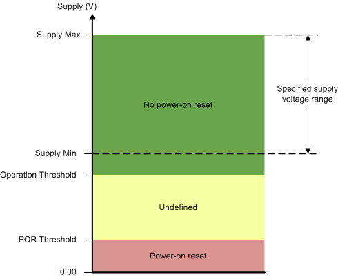
The DACx1001 incorporate two internal POR circuits for the DVDD, AVDD, IOVDD, VCC, and VSS supplies. The POR signals are ANDed together, so that all supplies must be at the minimal specified values for the device to not be in a reset condition. These POR circuits initialize internal registers, as well as set the analog outputs to a known state while the device supplies are ramping. All registers are reset to default values. The DACx1001 power on with the DAC registers set to zero scale. The DAC can be powered down by writing 1 to PDN (bit 4, address 02h). Typically, the POR function can be ignored as long as the device supplies power up and maintain the specified minimum voltage levels. However, in the case of supply drop or brownout, the DACx1001 can have an internal POR reset event. Figure 45 represents the internal POR threshold levels for the DVDD, AVDD, IOVDD, VCC, and VSS supplies.
 Figure 45. Relevant Voltage Levels for the POR Circuit
 For the DVDD supply, no internal POR occurs for nominal supply operation from 2.7 V (supply minimum) to 5.5 V (supply maximum). For a DVDD supply region between 2.5 V (undefined operation threshold) and 1.6 V (POR threshold), the internal POR circuit may or may not provide a reset over all temperature conditions. For a DVDD supply less than 1.6 V (POR threshold), the internal POR resets as long as the supply voltage is less than 1.6 V for approximately 1 ms.
For the AVDD supply, no internal POR occurs for nominal supply operation from 4.5 V (supply minimum) to 5.5 V (supply maximum). For an AVDD supply region between 4.1 V (undefined operation threshold) and 3.3 V (POR threshold), the internal POR circuit may or may not provide a reset over all temperature conditions. For an AVDD supply less than 3.3 V (POR threshold), the internal POR resets as long as the supply voltage is less than 3.3 V for approximately 1 ms.
For the VCC supply, no internal POR occurs for nominal supply operation from 8 V (supply minimum) to 36 V (supply maximum). For VCC supply voltages between 7.5 V (undefined operation threshold) to 6 V (POR threshold), the internal POR circuit may or may not provide a reset over all temperature conditions. For a VCC supply less than 6 V (POR threshold), the internal POR resets as long as the supply voltage is less than 6 V for approximately 1 ms.
For the VSS supply, no internal POR occurs for nominal supply operation from –3 V (supply minimum) to –18 V (supply maximum). For VSS supply voltages between –2.7 V (undefined operation threshold) to –1.8 V (POR threshold), the internal POR circuit may or may not provide a reset over all temperature conditions. For a VSS supply greater than –1.8 V (POR threshold), the internal POR resets as long as the supply voltage is greater than –1.8 V for approximately 1 ms.
For the IOVDD supply, no internal POR occurs for nominal supply operation from 1.8 V (supply minimum) to 5.5 V (supply maximum). For IOVDD supply voltages between 1.5 V (undefined operation threshold) and 0.8 V (POR threshold), the internal POR circuit may or may not provide a reset over all temperature conditions. For an IOVDD supply less than 0.8 V (POR threshold), the internal POR resets as long as the supply voltage is less than 0.8 V for approximately 1 ms.
In case the DVDD, AVDD, IOVDD, VCC, or VSS supply drops to a level where the internal POR signal is indeterminate, power cycle the device followed by a software reset.