SBAS649B June   2021  – June 2022 DAC12DL3200

PRODUCTION DATA  

  1. Features
  2. Applications
  3. Description
  4. Revision History
  5. Pin Configuration and Functions
  6. Specifications
    1. 6.1  Absolute Maximum Ratings
    2. 6.2  ESD Ratings
    3. 6.3  Recommended Operating Conditions
    4. 6.4  Thermal Information
    5. 6.5  Electrical Characteristics - DC Specifications
    6. 6.6  Electrical Characteristics - Power Consumption
    7. 6.7  Electrical Characteristics - AC Specifications
    8. 6.8  Timing Requirements
    9. 6.9  Switching Characteristics
    10. 6.10 Typical Characteristics
  7. Detailed Description
    1. 7.1 Overview
    2. 7.2 Functional Block Diagram
    3. 7.3 Feature Description
      1. 7.3.1 DAC Output Modes
        1. 7.3.1.1 NRZ Mode
        2. 7.3.1.2 RTZ Mode
        3. 7.3.1.3 RF Mode
        4. 7.3.1.4 2xRF Mode
      2. 7.3.2 DAC Output Interface
        1. 7.3.2.1 DAC Output Structure
        2. 7.3.2.2 Full-scale Current Adjustment
        3. 7.3.2.3 Example Analog Output Interfaces
      3. 7.3.3 LVDS Interface
        1. 7.3.3.1 MODE0: Two LVDS banks per channel
        2. 7.3.3.2 MODE1: One LVDS bank per channel
        3. 7.3.3.3 MODE2: Four LVDS banks, single channel mode
        4. 7.3.3.4 LVDS Interface Input Strobe
        5. 7.3.3.5 FIFO Operation
          1. 7.3.3.5.1 Using FIFO Delay Readback Values
          2. 7.3.3.5.2 FIFO Delay Handling
          3. 7.3.3.5.3 FIFO Delay and NCO Operation
          4. 7.3.3.5.4 FIFO Over/Under Flow Alarming
      4. 7.3.4 Multi-Device Synchronization (SYSREF+/-)
        1. 7.3.4.1 DACCLK Domain Synchronization
        2. 7.3.4.2 SYSREF Position Detector and Sampling Position Selection (SYSREF Windowing)
      5. 7.3.5 Alarms
    4. 7.4 Device Functional Modes
      1. 7.4.1 Direct Digital Synthesis (DDS) Mode
        1. 7.4.1.1 NCO Gain Scaling
        2. 7.4.1.2 NCO Phase Continuous Operation
        3. 7.4.1.3 Trigger Clock
    5. 7.5 Programming
      1. 7.5.1 Using the Serial Interface
        1. 7.5.1.1 SCS
        2. 7.5.1.2 SCLK
        3. 7.5.1.3 SDI
        4. 7.5.1.4 SDO
        5. 7.5.1.5 Serial Interface Operation
        6. 7.5.1.6 Streaming Mode
      2. 7.5.2 SPI Register Map
  8. Application and Implementation
    1. 8.1 Application Information
      1. 8.1.1 Startup Procedure with LVDS Input
      2. 8.1.2 Startup Procedure With NCO Operation
      3. 8.1.3 Interface Test Pattern and Timing Verification
    2. 8.2 Typical Application
      1. 8.2.1 Design Requirements
      2. 8.2.2 Detailed Design Procedure
      3. 8.2.3 Application Curves
    3. 8.3 Power Supply Recommendations
      1. 8.3.1 Power Up and Down Sequence
    4. 8.4 Layout
      1. 8.4.1 Layout Guidelines
      2. 8.4.2 Layout Example
  9. Device and Documentation Support
    1. 9.1 Receiving Notification of Documentation Updates
    2. 9.2 Support Resources
    3. 9.3 Trademarks
    4. 9.4 Electrostatic Discharge Caution
    5. 9.5 Glossary
  10. 10Mechanical, Packaging, and Orderable Information

Package Options

Mechanical Data (Package|Pins)
Thermal pad, mechanical data (Package|Pins)
Orderable Information

2xRF Mode

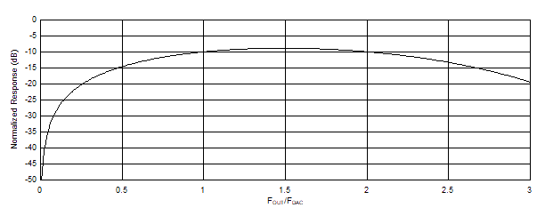
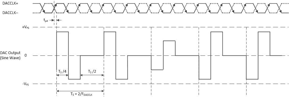
2xRF mode is a combination of RF mode (return to complement) for the first half of the sample period and a return-to-zero for the second half of the sample period. The result is a sinc response that peaks and provides maximum flatness in the 3rd, 4th and 5th Nyquist zones. 2xRF mode is only available in dual channel mode and requires an input clock at twice the DAC sample rate. The timing diagram for 2xRF mode is given in Figure 7-7. A plot of the frequency response of RF mode is shown in Figure 7-8.
GUID-5186F00E-59C5-46F4-A905-7DEA6E5D27F1-low.gifFigure 7-7 2xRF Mode Timing Diagram
GUID-8E0852EA-1B42-491D-9438-E73DBCBE8745-low.gifFigure 7-8 2xRF Mode Output Waveform Frequency Response