SBAS649B June   2021  – June 2022 DAC12DL3200

PRODUCTION DATA  

  1. Features
  2. Applications
  3. Description
  4. Revision History
  5. Pin Configuration and Functions
  6. Specifications
    1. 6.1  Absolute Maximum Ratings
    2. 6.2  ESD Ratings
    3. 6.3  Recommended Operating Conditions
    4. 6.4  Thermal Information
    5. 6.5  Electrical Characteristics - DC Specifications
    6. 6.6  Electrical Characteristics - Power Consumption
    7. 6.7  Electrical Characteristics - AC Specifications
    8. 6.8  Timing Requirements
    9. 6.9  Switching Characteristics
    10. 6.10 Typical Characteristics
  7. Detailed Description
    1. 7.1 Overview
    2. 7.2 Functional Block Diagram
    3. 7.3 Feature Description
      1. 7.3.1 DAC Output Modes
        1. 7.3.1.1 NRZ Mode
        2. 7.3.1.2 RTZ Mode
        3. 7.3.1.3 RF Mode
        4. 7.3.1.4 2xRF Mode
      2. 7.3.2 DAC Output Interface
        1. 7.3.2.1 DAC Output Structure
        2. 7.3.2.2 Full-scale Current Adjustment
        3. 7.3.2.3 Example Analog Output Interfaces
      3. 7.3.3 LVDS Interface
        1. 7.3.3.1 MODE0: Two LVDS banks per channel
        2. 7.3.3.2 MODE1: One LVDS bank per channel
        3. 7.3.3.3 MODE2: Four LVDS banks, single channel mode
        4. 7.3.3.4 LVDS Interface Input Strobe
        5. 7.3.3.5 FIFO Operation
          1. 7.3.3.5.1 Using FIFO Delay Readback Values
          2. 7.3.3.5.2 FIFO Delay Handling
          3. 7.3.3.5.3 FIFO Delay and NCO Operation
          4. 7.3.3.5.4 FIFO Over/Under Flow Alarming
      4. 7.3.4 Multi-Device Synchronization (SYSREF+/-)
        1. 7.3.4.1 DACCLK Domain Synchronization
        2. 7.3.4.2 SYSREF Position Detector and Sampling Position Selection (SYSREF Windowing)
      5. 7.3.5 Alarms
    4. 7.4 Device Functional Modes
      1. 7.4.1 Direct Digital Synthesis (DDS) Mode
        1. 7.4.1.1 NCO Gain Scaling
        2. 7.4.1.2 NCO Phase Continuous Operation
        3. 7.4.1.3 Trigger Clock
    5. 7.5 Programming
      1. 7.5.1 Using the Serial Interface
        1. 7.5.1.1 SCS
        2. 7.5.1.2 SCLK
        3. 7.5.1.3 SDI
        4. 7.5.1.4 SDO
        5. 7.5.1.5 Serial Interface Operation
        6. 7.5.1.6 Streaming Mode
      2. 7.5.2 SPI Register Map
  8. Application and Implementation
    1. 8.1 Application Information
      1. 8.1.1 Startup Procedure with LVDS Input
      2. 8.1.2 Startup Procedure With NCO Operation
      3. 8.1.3 Interface Test Pattern and Timing Verification
    2. 8.2 Typical Application
      1. 8.2.1 Design Requirements
      2. 8.2.2 Detailed Design Procedure
      3. 8.2.3 Application Curves
    3. 8.3 Power Supply Recommendations
      1. 8.3.1 Power Up and Down Sequence
    4. 8.4 Layout
      1. 8.4.1 Layout Guidelines
      2. 8.4.2 Layout Example
  9. Device and Documentation Support
    1. 9.1 Receiving Notification of Documentation Updates
    2. 9.2 Support Resources
    3. 9.3 Trademarks
    4. 9.4 Electrostatic Discharge Caution
    5. 9.5 Glossary
  10. 10Mechanical, Packaging, and Orderable Information

Package Options

Mechanical Data (Package|Pins)
Thermal pad, mechanical data (Package|Pins)
Orderable Information

Direct Digital Synthesis (DDS) Mode

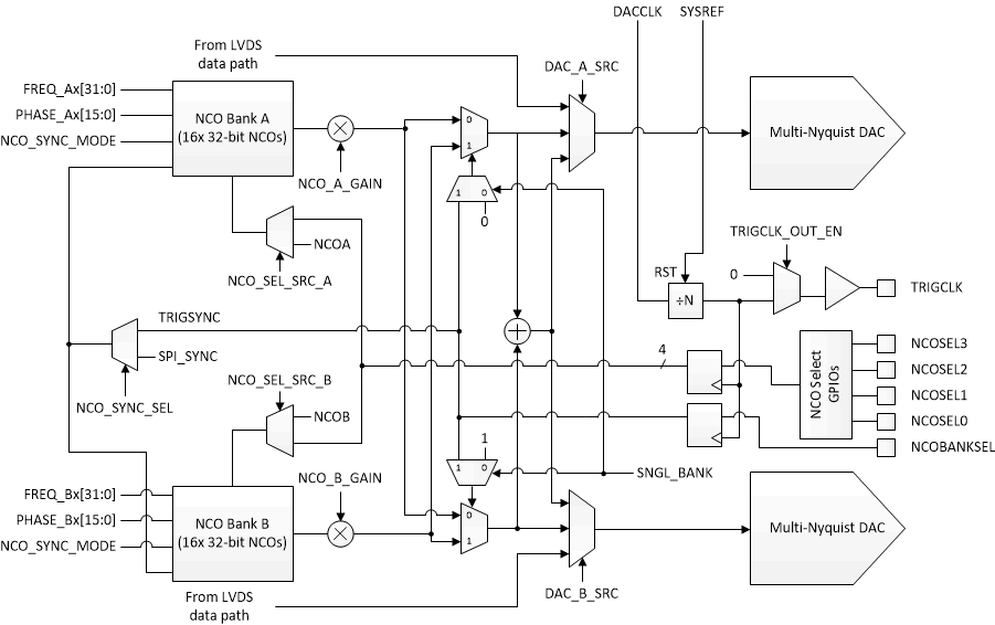
The DAC12DL3200 contains two numerically controlled oscillators (NCOs) that can optionally be used for direct digital synthesis of tones for each DAC. The block diagram for the DDS is shown in Figure 7-22. There are two NCO banks, each with 16 separate 32-bit NCOs. The banks can be used separately for each DAC, or together to provide 32 NCOs for one DAC. The two NCOs can be summed as a two tone source for one DAC. The NCO can be selected either through registers NCO_SEL_A and NCO_SEL_B, or through balls NCOSEL[0:3] and NCOBANKSEL.
GUID-A3DD120C-CA1C-4C2C-AA18-FF939FDB053C-low.gifFigure 7-22 DDS Block Diagram